

| Distributor | Stock | Pricing | MOQ | PKG | Lead Time | Date Code | On Order Quantity | On Order Delivery | |
|---|---|---|---|---|---|---|---|---|---|
|
146 pcs
|
146 pcs | On Request | 1 | On Request | On Request | On Request | On Request | On Request | |
|
6 pcs
|
6 pcs | On Request | 1 | On Request | On Request | On Request | On Request | On Request |
| Category | |
| Manufacturer Name | |
| AEC Qualified | |
| Automotive Grade | |
| Capacitance | |
| Clock Frequency | |
| Current | |
| Data Rate (Max) | |
| Delay Time | |
| ESD Protection | |
| Function | |
| Industrial Grade | |
| Input | |
| Input Signal | |
| Lead Spacing | |
| Medical Grade | |
| Military Grade | |
| Mounting Type | |
| Number of Channels | |
| Operating Temperature | |
| Output | |
| Output Signal | |
| Power Dissipation | |
| Propagation Delay | |
| Supplier Device Package | |
| Supplier Package | |
| Type | |
| Voltage |
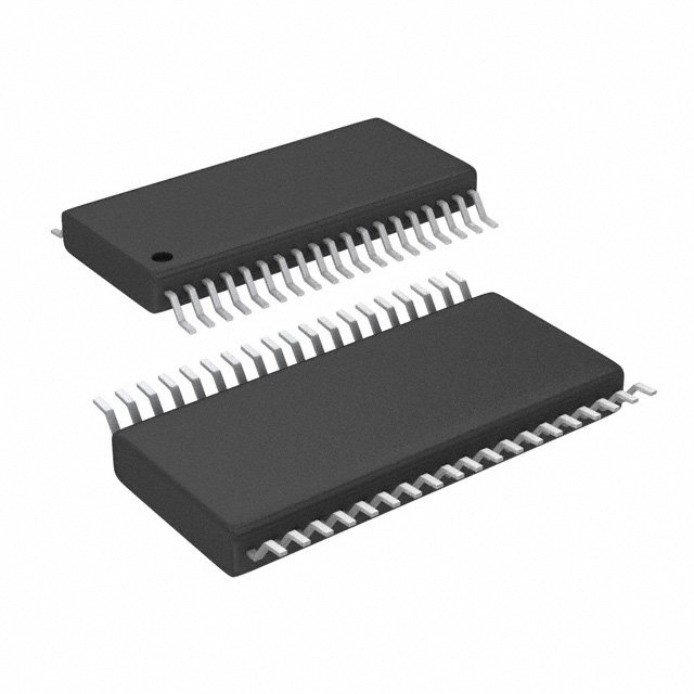
The SN65LVDS108DBT from Texas Instruments is an 8-port LVDS clock fanout buffer designed for high-speed signal distribution. This device functions as a receiver and repeater, supporting LVDS protocols with a typical signaling rate of up to 400 Mbps or clock frequencies up to 400 MHz.
Key electrical specifications include an operating voltage range of 3V to 3.6V, a propagation delay of less than 4.7 ns, and output skew under 300 ps. The buffer offers individual control for each driver output and is compatible with various logic levels when external termination networks are used. It is packaged in a 38-TSSOP surface mount configuration.
This repeater meets or exceeds the requirements of the ANSI EIA/TIA-644 standard. It is suitable for applications requiring reliable distribution of high-frequency clock signals. The device also features bus-pin ESD protection exceeding 12 kV.
| Qty | Low | High |
|---|---|---|
| 1+ | $3.87 | $3.87 |
Estimated market price range - modelled values for guidance only, not live distributor offers.
The signaling rate is up to 400 Mbps.
The operating temperature range is -40°C to 85°C.
It is available in a 38-TSSOP package.
The operating voltage is between 3V and 3.6V.
The propagation delay is less than 4.7 ns.
The output skew is less than 300 ps.