

| Distributor | Stock | Pricing | MOQ | PKG | Lead Time | Date Code | On Order Quantity | On Order Delivery | |
|---|---|---|---|---|---|---|---|---|---|
|
5,765 pcs
|
5765 pcs | On Request | 1 | On Request | On Request | On Request | On Request | On Request |
| Category | |
| Manufacturer Name |
The SN65LVDS105 from Texas Instruments is a versatile clock fanout buffer that implements the electrical characteristics of low-voltage differential signaling (LVDS). This device is designed to receive a single LVTTL input signal and distribute it to four LVDS outputs, making it suitable for high-speed clock distribution applications.
With a typical data signaling rate of up to 400 Mbps or clock frequencies up to 400 MHz, the SN65LVDS105 is ideal for systems requiring precise clock synchronization. It operates from a single 3.3-V supply and offers a low-voltage differential signaling output with a typical voltage of 350 mV into a 100-ohm load. The propagation delay is a mere 2.2 ns (typical), ensuring minimal skew in clock signals.
The device meets or exceeds the requirements of the ANSI EIA/TIA-644 standard for LVDS. The LVTTL inputs are 5-V tolerant, providing flexibility in interfacing with different logic levels. Driver outputs are high-impedance when disabled or when the supply voltage drops below 1.5 V. Bus-pin ESD protection exceeds 16 kV, enhancing robustness.
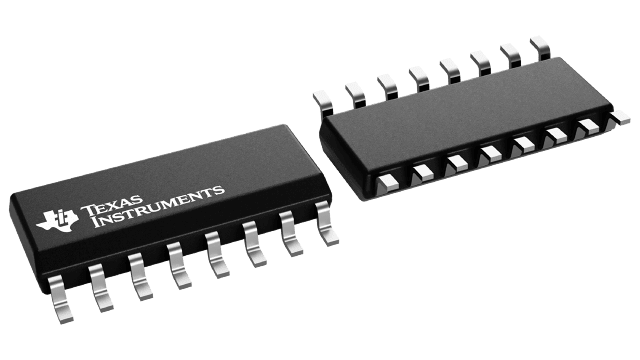
The SN65LVDS105 is available in SOIC and TSSOP packages, supporting various board space requirements. Its operating temperature range is from -40°C to 85°C, making it suitable for a wide range of industrial and commercial applications.
| Qty | Low | High |
|---|---|---|
| 1+ | $3.00 | $3.00 |
Estimated market price range - modelled values for guidance only, not live distributor offers.
The device operates from a single 3.3 V supply.
Available in SOIC (D) 16 and TSSOP (PW) 16 packages.
The operating temperature range is -40°C to 85°C.
The typical signaling rate is 400 Mbps.
It has 4 transmitters and 1 receiver.
The bus-pin ESD protection exceeds 16 kV.
The typical propagation delay is 2.2 ns.