

| Distributor | Stock | Pricing | MOQ | PKG | Lead Time | Date Code | On Order Quantity | On Order Delivery | |
|---|---|---|---|---|---|---|---|---|---|
|
2,800 pcs
|
2800 pcs | On Request | 1 | On Request | On Request | On Request | On Request | On Request | |
|
1,638 pcs
|
1638 pcs | On Request | 1 | On Request | On Request | On Request | On Request | On Request | |
|
55 pcs
|
55 pcs | On Request | 1 | On Request | On Request | On Request | On Request | On Request |
| Category | |
| Manufacturer Name | |
| AEC Qualified | |
| Automotive Grade | |
| Capacitance | |
| Current | |
| Data Rate (Max) | |
| Delay Time | |
| Industrial Grade | |
| Input | |
| Input Signal Type | |
| Lead Spacing | |
| Medical Grade | |
| Military Grade | |
| Mounting Type | |
| Number of Channels | |
| Operating Temperature | |
| Operating Voltage | |
| Output | |
| Output Signal Type | |
| Supplier Device Package | |
| Type | |
| Voltage | |
| data_rate_max (Maximum) | |
| propagation_delay_time (Typical @ Typical) |
The SN65LVDS104PW from Texas Instruments is a versatile 1:4 LVDS clock fanout buffer. This component is engineered to receive LVDS input signals and distribute them to four LVDS outputs, supporting data signaling rates up to 400 Mbps or clock frequencies up to 400 MHz.
Key electrical characteristics include a typical propagation delay of 3.1 ns and operation from a single 3.3V supply. The device is designed to meet or exceed the requirements of the ANSI EIA/TIA-644 standard for Low-Voltage Differential Signaling (LVDS).
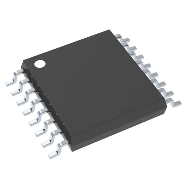
The SN65LVDS104PW is available in a compact 16-TSSOP package, suitable for surface mount applications. Its operating temperature range is -40°C to 85°C, making it suitable for a variety of environmental conditions. The component's ability to interface with multiple signaling standards, including LVPECL, LVTTL, and LVCMOS with external networks, adds to its design flexibility.
| Qty | Low | High |
|---|---|---|
| 1+ | $3.21 | $3.21 |
Estimated market price range - modelled values for guidance only, not live distributor offers.
The SN65LVDS104PW supports data signaling rates up to 400 Mbps.
The typical propagation delay for the SN65LVDS104PW is 3.1 ns.
The SN65LVDS104PW operates from a single 3.3V supply.
The SN65LVDS104PW operates within a temperature range of -40°C to 85°C.
The SN65LVDS104PW is available in a 16-TSSOP package.
The SN65LVDS104PW accepts LVDS input signals.
The SN65LVDS104PW supports output signals including BTL, CTT, GTL, HSTL, LVCMOS, LVDS, LVPECL, LVTTL, PECL, and SSTL.