

| Distributor | Stock | Pricing | MOQ | PKG | Lead Time | Date Code | On Order Quantity | On Order Delivery | |
|---|---|---|---|---|---|---|---|---|---|
|
47 pcs
|
47 pcs | On Request | 1 | On Request | On Request | On Request | On Request | On Request |
| Category | |
| Manufacturer Name |
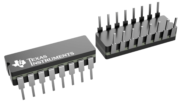
The SN55LBC175J from Texas Instruments is a monolithic quadruple differential line receiver with 3-state outputs. It is designed to meet EIA Standards RS-422-A, RS-423-A, RS-485, and CCITT V.11, making it suitable for balanced multipoint bus transmission in noisy environments.
This device supports data rates up to and exceeding 10 million bits per second. The receivers are enabled in pairs with an active-high enable input. Each receiver input offers high impedance, hysteresis for enhanced noise immunity, and a sensitivity of ±200 mV over a common-mode input voltage range of -7 V to 12 V. The fail-safe design ensures that outputs remain high if inputs are open-circuited.
Key electrical specifications include a maximum supply current of 11000 µA and a maximum signaling rate of 10 Mbps. It operates within a military temperature range of -55°C to 125°C. The SN55LBC175J is designed for multipoint transmission on long bus lines and is built using Texas Instruments' LinBiCMOS technology for low power consumption and high switching speeds.
Available in LCCC (FK), CDIP (J), and CFP (W) package types, this receiver is optimized for robust performance in demanding applications.
| Qty | Low | High |
|---|---|---|
| 1+ | $46.81 | $46.81 |
Estimated market price range - modelled values for guidance only, not live distributor offers.
The SN55LBC175J has 4 receivers.
The maximum signaling rate is 10 Mbps.
The operating temperature range is -55°C to 125°C.
Fault protection is from -10 V to 15 V.
The common-mode input voltage range is -7 V to 12 V.
It supports up to 32 nodes.
Available packages include LCCC (FK), CDIP (J), and CFP (W).