

| Distributor | Stock | Pricing | MOQ | PKG | Lead Time | Date Code | On Order Quantity | On Order Delivery | |
|---|---|---|---|---|---|---|---|---|---|
|
96,758 pcs
|
96758 pcs | On Request | 1 | On Request | On Request | 18+ | On Request | On Request | |
|
61,020 pcs
|
61020 pcs | On Request | 1 | On Request | On Request | On Request | On Request | On Request | |
|
355 pcs
|
355 pcs | On Request | 1 | On Request | On Request | On Request | On Request | On Request |
| Category | |
| Manufacturer Name | |
| Current | |
| DC Current Gain (hFE) (Min) @ Ic, Vce | |
| Halogen Free | |
| Mounting Type | |
| Power | |
| Resistor | |
| Supplier Device Package | |
| Transistor Type | |
| Vce Saturation (Max) @ Ib, Ic | |
| Voltage |
The SMUN5235DW1T1G is a Dual NPN Bias Resistor Transistor (BRT) manufactured by ON Semiconductor. This integrated device simplifies circuit design by combining a single transistor with a monolithic bias network, eliminating the need for external resistors. It offers a collector-emitter voltage (VCEO) of 50V and a continuous collector current (IC) of 100mA.
The transistor features two NPN transistors with integrated bias resistors, including a series base resistor and a base-emitter resistor. The internal resistors are specified as R1 = 2.2 kΩ and R2 = 47 kΩ. The device has a maximum input forward voltage of 12Vdc and a maximum input reverse voltage of 5Vdc.
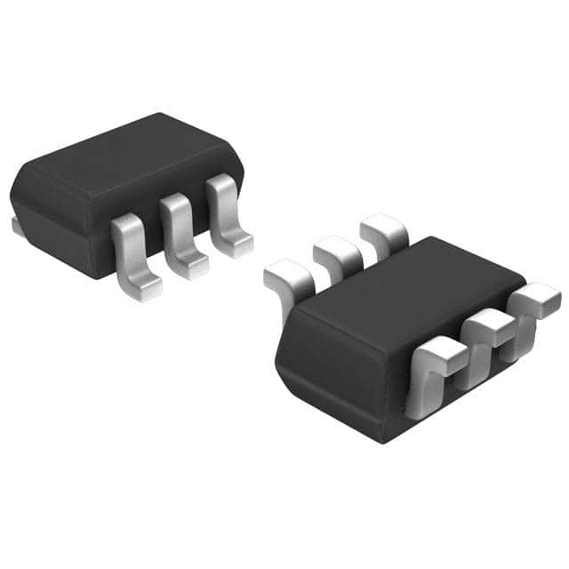
This component is supplied in a SOT-363 package, also known as SC-88 or SC70-6, and is designed for surface mount applications. The power dissipation is rated at 187mW at 25°C ambient temperature for a single junction heated, and 250mW for both junctions heated. The device is Pb-Free, Halogen Free/BFR Free, and RoHS Compliant.
Key electrical characteristics include a minimum DC current gain (hFE) of 80 at 5mA/10V and a saturation voltage (Vce(sat)) of 250mV at 1mA/10mA. The SMUN5235DW1T1G is suitable for applications requiring reduced component count and board space.
| Qty | Low | High |
|---|---|---|
| 1+ | $0.99 | $0.99 |
Estimated market price range - modelled values for guidance only, not live distributor offers.
50 Vdc.
SOT-363 (also known as SC-88/SC70-6), surface mount.
Minimum 80 at 5 mA collector current and 10 V collector-emitter voltage.
Maximum 250 mV at 1 mA base current and 10 mA collector current.
Maximum input forward voltage is 12 Vdc, maximum input reverse voltage is 5 Vdc.
Total device dissipation: 187 mW (Note 1) and 256 mW (Note 2) for individual transistors; 250 mW (Note 1) and 385 mW (Note 2) when both junctions are heated at 25°C ambient.
R1 = 2.2 kΩ, R2 = 47 kΩ.