

| Distributor | Stock | Pricing | MOQ | PKG | Lead Time | Date Code | On Order Quantity | On Order Delivery | |
|---|---|---|---|---|---|---|---|---|---|
|
36,160 pcs
|
36160 pcs | On Request | 1 | On Request | On Request | On Request | On Request | On Request |
| Category | |
| Manufacturer Name | |
| Current | |
| Drain to Source Voltage (Vdss) | |
| Drive Voltage (Max Rds On, Min Rds On) | |
| FET Type | |
| Gate Charge (Qg) (Max) @ Vgs | |
| Halogen Free | |
| Input Capacitance (Ciss) (Max) @ Vds | |
| Mounting Type | |
| Operating Temperature | |
| Power Dissipation (Max) | |
| Rds On (Max) @ Id, Vgs | |
| Supplier Device Package | |
| Supplier Package | |
| Technology | |
| Vgs (Max) | |
| Vgs(th) (Max) @ Id |
The Vishay Dale SIR876DP-T1-GE3 is an N-Channel MOSFET designed for various applications including DC/DC primary side switching, telecom/server 48V systems, and industrial use. It features a 100V drain-source breakdown voltage and a continuous drain current rating of 40A at 25°C case temperature.
This MOSFET offers a low on-resistance (Rds On) of 10.8mOhm at 20A and 10V gate-source voltage. It operates within a junction temperature range of -55°C to 150°C and has a maximum power dissipation of 62.5W at 25°C case temperature and 5W at 25°C ambient temperature. The device is built using TrenchFET technology and is tested to 100% Rg and 100% UIS standards.
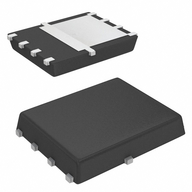
The SIR876DP-T1-GE3 is supplied in a PowerPAK SO-8 surface-mount package. It is compliant with RoHS Directive 2002/95/EC and is halogen-free according to IEC 61249-2-21 definition. The component is classified as obsolete, making substitute parts essential for design continuity.
| Qty | Low | High |
|---|---|---|
| 1+ | $0.99 | $0.99 |
Estimated market price range - modelled values for guidance only, not live distributor offers.
The minimum drain-source breakdown voltage is 100V at VGS=0V, ID=250µA.
The maximum continuous drain current is 40A at case temperature 25°C, and 15.2A at ambient temperature 25°C.
The operating junction and storage temperature range is -55°C to 150°C.
The device is supplied in a PowerPAK® SO-8 surface-mount package.
The typical gate charge is 16.9nC at VGS=10V. The maximum gate charge is 48nC at VGS=10V.
The maximum on-resistance is 10.8mΩ at VGS=10V, ID=20A. Typical values are 10.8mΩ at 10V, 11.4mΩ at 7.5V, and 14.5mΩ at 4.5V.
Yes, the device is 100% UIS tested with a single-pulse avalanche energy rating of 31.2mJ and avalanche current of 25A.