

| Distributor | Stock | Pricing | MOQ | PKG | Lead Time | Date Code | On Order Quantity | On Order Delivery | |
|---|---|---|---|---|---|---|---|---|---|
|
400 pcs
|
400 pcs | On Request | 1 | On Request | On Request | On Request | On Request | On Request |
| Category | |
| Manufacturer Name | |
| Differential | |
| Divider | |
| Frequency | |
| Input | |
| Mounting Type | |
| Number of Circuits | |
| Operating Temperature | |
| Output | |
| PLL | |
| Phase Jitter | |
| Ratio | |
| Supplier Device Package | |
| Tape & Reel | |
| Type | |
| Voltage |
The Skyworks Solutions SI5397J-A11023-GM is a high-performance, 8-output jitter-attenuating clock multiplier. It integrates four any-frequency DSPLLs for applications requiring maximum integration and independent timing paths. This device provides any-frequency conversion with typical jitter performance of 95 fs.
Key electrical specifications include an input frequency range of 8 kHz to 750 MHz (Differential) and 8 kHz to 250 MHz (LVCMOS). The output frequency range is 100 Hz to 720 MHz (Differential) and 100 Hz to 250 MHz (LVCMOS). It operates at voltages between 1.71V and 3.47V and has a maximum frequency of 720 MHz.
This jitter attenuator supports independent free-run and holdover modes of operation, as well as automatic and hitless input clock switching. It is programmable via a serial interface with in-circuit programmable non-volatile memory, ensuring it powers up in a known configuration. Programming is facilitated by Skyworks' ClockBuilder Pro software.
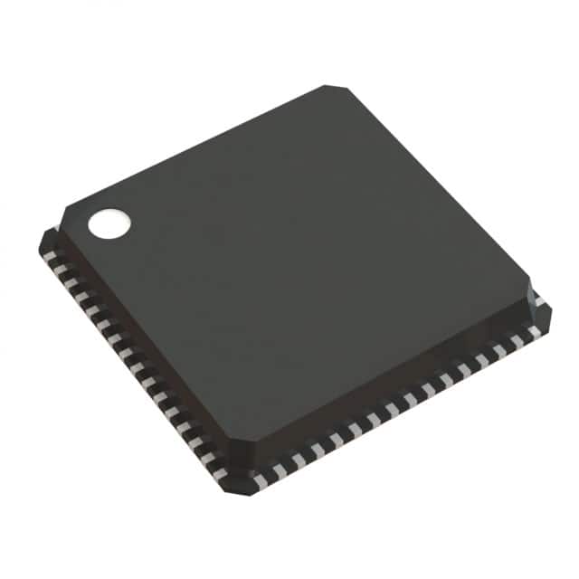
The SI5397J-A11023-GM is available in a 64-VFQFN Exposed Pad package and is designed for surface mount applications. Its operating temperature range is -40°C to 85°C (TA).
| Qty | Low | High |
|---|---|---|
| 1+ | $7.01 | $7.01 |
Estimated market price range - modelled values for guidance only, not live distributor offers.
The maximum output frequency is 720 MHz for differential signals and 250 MHz for LVCMOS signals.
The operating temperature range is -40°C to 85°C (TA).
It is supplied in a 64-VFQFN Exposed Pad package.
The input frequency range is 8 kHz to 750 MHz for differential signals and 8 kHz to 250 MHz for LVCMOS signals.
The typical phase jitter performance is 95 fs rms.
Supported output types include CML, HCSL, LVCMOS, LVDS, and LVPECL.