

| Distributor | Stock | Pricing | MOQ | PKG | Lead Time | Date Code | On Order Quantity | On Order Delivery | |
|---|---|---|---|---|---|---|---|---|---|
|
4,020 pcs
|
4020 pcs | On Request | 1 | On Request | On Request | 16+ | On Request | On Request |
| Category | |
| Manufacturer Name | |
| Current | |
| Drain to Source Voltage (Vdss) | |
| Drive Voltage (Max Rds On, Min Rds On) | |
| FET Type | |
| Gate Charge (Qg) (Max) @ Vgs | |
| Halogen Free | |
| Mounting Type | |
| Operating Temperature | |
| Power Dissipation (Max) | |
| Rds On (Max) @ Id, Vgs | |
| Supplier Device Package | |
| Supplier Package | |
| Technology | |
| Vgs (Max) | |
| Vgs(th) (Max) @ Id |
The Vishay Dale SI4403BDY-T1-E3 is a P-Channel MOSFET designed for various electronic applications. It features a maximum Drain-Source Voltage (Vds) of 20V and a continuous drain current (Id) of 7.3A at 25°C.
The MOSFET offers a low on-state resistance (Rds(on)) as low as 0.017Ω at 4.5V Vgs and 9.9A Id. Its Gate Threshold Voltage (Vgs(th)) is a maximum of 1V at 350µA. The device operates within a temperature range of -55°C to 150°C.
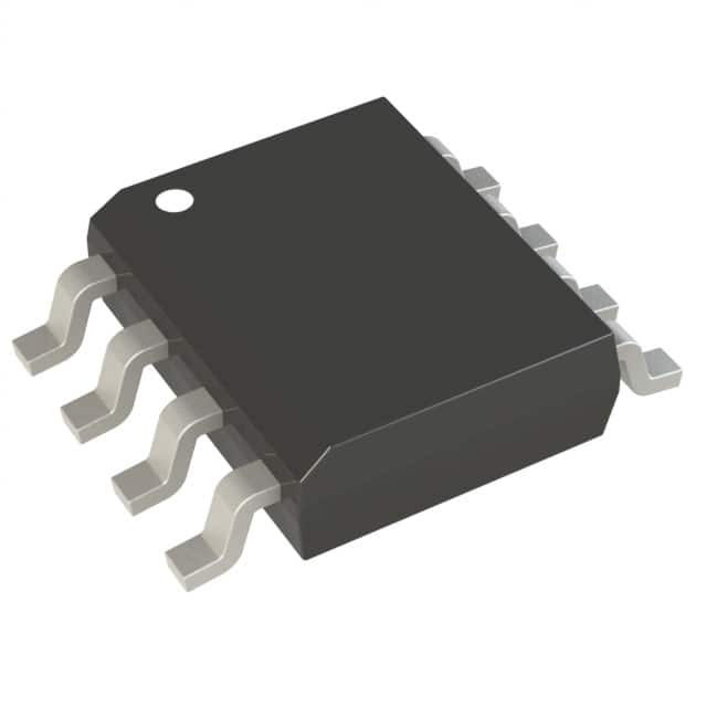
Packaged in an 8-SOIC (Small Outline Integrated Circuit) package, the SI4403BDY-T1-E3 is suitable for surface mounting. Its dimensions and gull wing terminal form facilitate integration into standard PCB layouts. The power dissipation is rated at 1.35W at 25°C ambient temperature.
This MOSFET is compliant with RoHS3 standards and has a Moisture Sensitivity Level (MSL) of 1. It is also described as Halogen-free and Lead (Pb)-free, aligning with environmental regulations.
| Qty | Low | High |
|---|---|---|
| 1+ | $0.99 | $0.99 |
Estimated market price range - modelled values for guidance only, not live distributor offers.
The maximum drain-source voltage is -20 V.
The device is supplied in an 8-SOIC (0.154", 3.90mm Width) surface mount package.
The operating junction temperature range is -55°C to 150°C.
The maximum continuous drain current is 9.9 A at 25°C ambient temperature.
The on-resistance is 0.017 Ω at VGS = -4.5 V and ID = -9.9 A.
The gate threshold voltage is 1 V maximum at VDS = VGS and ID = -350 µA.
The total gate charge is 50 nC at VDS = -10 V, VGS = -5 V, and ID = -9.9 A.