

| Distributor | Stock | Pricing | MOQ | PKG | Lead Time | Date Code | On Order Quantity | On Order Delivery | |
|---|---|---|---|---|---|---|---|---|---|
|
15 pcs
|
15 pcs | On Request | 1 | On Request | On Request | 15+ | On Request | On Request |
| Category | |
| Manufacturer Name | |
| Clock Frequency | |
| Data Rate | |
| Operating Temperature | |
| Power Consumption |
The Texas Instruments SCAN921226HSM is a high-temperature 10-bit deserializer designed for interface applications. It operates within a clock frequency range of 20 to 80 MHz, supporting a serial data rate of 800 Mbps.
This device transforms a Bus LVDS serial data stream back into a 10-bit wide parallel data bus and recovers the parallel clock. It is compliant with IEEE 1149.1 Standard for Boundary Scan Test, providing access via a standard Test Access Port (TAP) for verifying differential signal integrity. The SCAN921226HSM also features an at-speed BIST mode.
Key electrical characteristics include a typical power consumption of less than 600 mW at 80 MHz. The parallel interface is 10-bit, accommodating 1 byte of data plus 2 control bits. The operating temperature range is -40 to 125°C.
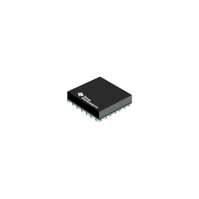
The SCAN921226HSM is housed in a compact 49-lead NFBGA package measuring 7 mm x 7 mm. Receiver inputs have high impedance when power is off, and the serial output is rated for a 27Ω load.
| Qty | Low | High |
|---|---|---|
| 1+ | $9.76 | $9.76 |
Estimated market price range - modelled values for guidance only, not live distributor offers.
The operating temperature range is -40 to 125°C.
The serial Bus LVDS data rate is 800 Mbps at an 80 MHz clock.
The SCAN921226HSM is available in a 49-lead NFBGA (NZA) package.
The parallel interface width is 10-bit.
The typical power consumption for the chipset (Tx + Rx) is less than 600 mW at 80 MHz.