

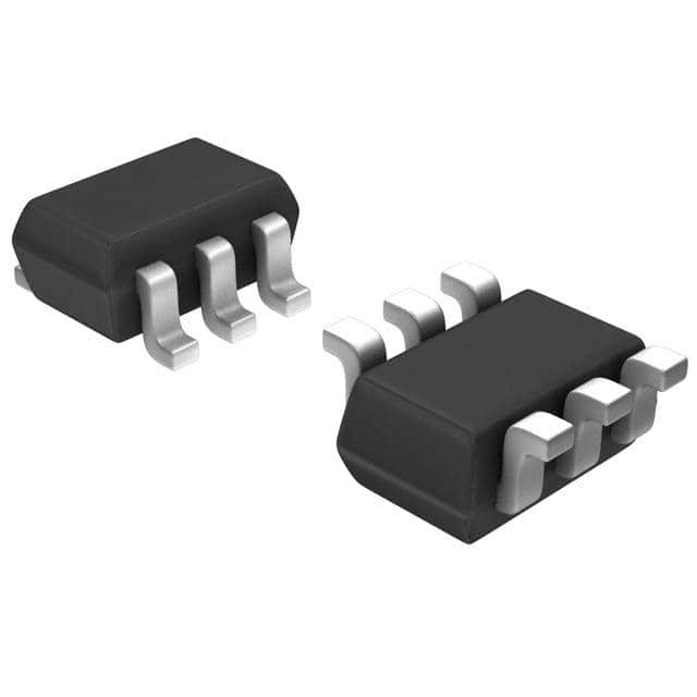
SBC857CDW1T1G The ON Semiconductor SBC857CDW1T1G is a PNP dual transistor array designed for general purpose amplifier applications. It features a 45V collector-emitter breakdown voltage and 100mA continuous collector current.
Mfr Part #:

SBC857CDW1T1G

Available from 1 distributors
Mfr Name: On Semiconductor
On Semiconductor
The ON Semiconductor SBC857CDW1T1G is a PNP dual transistor array designed for general purpose amplifier applications. It features a 45V collector-emitter breakdown voltage and 100mA continuous collector current.
✓ Total Stock: 75,000 pcs
$ Price Range: $0.99

SBC857CDW1T1G Available from 1 distributor

✓ Authorised
✓ Non-Authorised
Distributor Stock Pricing MOQ PKG Lead Time Date Code On Order Quantity On Order Delivery
Non-Authorised Inventory information
75,000 pcs
75000 pcs On Request 1 On Request On Request On Request On Request On Request

SBC857CDW1T1G Specifications Quick View

Most important parameters for selection – full specs in datasheet.
Category
Manufacturer Name
Current
DC Current Gain (hFE) (Min) @ Ic, Vce
Frequency
Halogen Free
Mounting Type
Operating Temperature
Power
Supplier Device Package
Transistor Type
Vce Saturation (Max) @ Ib, Ic
Voltage

SBC857CDW1T1G Description

Short technical summary and product information.

The ON Semiconductor SBC857CDW1T1G is a PNP dual transistor array housed in a compact SOT-363 (SC-88) surface mount package. This device is designed for general purpose amplifier applications and offers a collector-emitter breakdown voltage of 45V and a continuous collector current of 100mA.


Key electrical characteristics include a maximum power dissipation of 380mW and a transition frequency of 100MHz. The operating temperature range is from -55°C to 150°C. The transistor array is AEC-Q101 qualified and PPAP capable, making it suitable for automotive applications.


This component is Pb-Free, Halogen Free/BFR Free, and RoHS Compliant. Its surface mount package and dual PNP configuration make it a versatile choice for various electronic designs requiring amplification or switching functions.

SBC857CDW1T1G Quick Information

Product Type: PNP Dual Transistor Array
Series: Automotive, AEC-Q101
Canonical Name: On Semiconductor SBC857CDW1T1G PNP Dual Transistor Array
Subcategory: Bipolar (BJT)

SBC857CDW1T1G Compliance

RoHS Status: RoHS Compliant
Moisture Sensitivity Level (MSL): 1 Unlimited
REACH Status: REACH Unaffected

SBC857CDW1T1G Estimated Pricing

Qty Low High
1+ $0.99 $0.99

Estimated market price range - modelled values for guidance only, not live distributor offers.

SBC857CDW1T1G Features

  • Dual PNP transistor array configuration.
  • 45V collector-emitter breakdown voltage.
  • 100mA maximum continuous collector current.
  • 380mW maximum power dissipation.
  • AEC-Q101 qualified for automotive use.

SBC857CDW1T1G Applications

  • Suitable for general purpose amplification.
  • Designed for low power applications.
  • Automotive and other unique requirements.
  • Surface mount assembly compatibility.

SBC857CDW1T1G FAQs

7 frequently asked questions generated from this part’s specifications.
What is the maximum collector-emitter voltage (VCEO) of SBC857CDW1T1G?

The maximum collector-emitter voltage is -45V (45V absolute).

What is the package type of SBC857CDW1T1G?

The package is 6-TSSOP, SC-88, SOT-363; supplier device package is SC-88/SC70-6/SOT-363. Mounting type is surface mount.

What is the operating temperature range of SBC857CDW1T1G?

The operating temperature range is -55°C to 150°C (junction temperature).

What is the DC current gain (hFE) of SBC857CDW1T1G?

The minimum DC current gain (hFE) is 420 at Ic=2mA, Vce=5V.

What is the maximum power dissipation of SBC857CDW1T1G?

Maximum power dissipation is 380mW per device at TA=25°C.

What is the transition frequency (fT) of SBC857CDW1T1G?

The transition frequency is 100MHz.

Is the SBC857CDW1T1G lead-free and halogen-free?

Yes, it is verified Pb-free and halogen-free according to the datasheet.

Home
Account

Categories