

| Distributor | Stock | Pricing | MOQ | PKG | Lead Time | Date Code | On Order Quantity | On Order Delivery | |
|---|---|---|---|---|---|---|---|---|---|
|
1,455 pcs
|
1455 pcs | On Request | 1 | On Request | On Request | On Request | On Request | On Request |
| Category | |
| Manufacturer Name | |
| Applications | |
| Interface | |
| Lead Spacing | |
| Mounting Type | |
| Operating Temperature | |
| Operating Voltage | |
| Supplier Device Package | |
| Voltage |
The PX1011BI-EL1/G,557 from NXP Semiconductors is a high-performance, low-power, single-lane PCI Express electrical PHYsical layer (PHY). It handles the low-level PCI Express protocol and signaling, compliant with PCI Express Base Specification 1.1.
Key features include Clock and Data Recovery (CDR), data serialization and de-serialization (SerDes), 8b/10b encoding, and receiver detection. The device offers a 2.5 Gbit/s PCI Express lane and an 8-bit parallel data interface operating at 250 MHz with SSTL_2 signaling. It supports advanced power management functions and operates across an industrial temperature range of -40°C to +85°C.
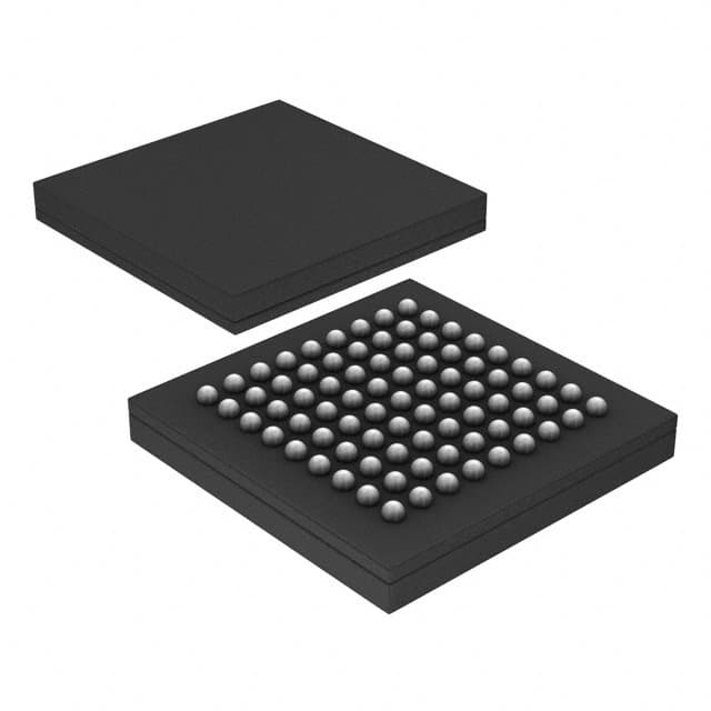
This PHY is designed for off-chip applications and is compatible with FPGA I/O interfaces. It also includes a JTAG (IEEE 1149.1) boundary scan interface and a Built-In Self Test (BIST) controller. The PX1011BI-EL1/G,557 is available in an 81-LFBGA package and is mounted via surface mount technology.
| Qty | Low | High |
|---|---|---|
| 1+ | $6.39 | $6.39 |
Estimated market price range - modelled values for guidance only, not live distributor offers.
The PX1011BI-EL1/G,557 is compliant to the PCI Express Base Specification 1.1.
The single PCI Express lane operates at 2.5 Gbit/s.
The 8-bit parallel data interface uses SSTL_2 Class I signaling.
The industrial operating temperature range is -40°C to +85°C.
The operating voltage is 1.2V.
It is supplied in an 81-LFBGA package.