

| Distributor | Stock | Pricing | MOQ | PKG | Lead Time | Date Code | On Order Quantity | On Order Delivery | |
|---|---|---|---|---|---|---|---|---|---|
|
500 pcs
|
500 pcs | On Request | 1 | On Request | On Request | On Request | On Request | On Request |
| Category | |
| Manufacturer Name | |
| Differential | |
| Frequency | |
| Input | |
| Input Type | |
| Mounting Type | |
| Number of Circuits | |
| Number of Inputs | |
| Operating Temperature | |
| Output | |
| Output Type | |
| Propagation Delay | |
| Ratio | |
| Supplier Device Package | |
| Supplier Package | |
| Tape & Reel | |
| Type | |
| Voltage |
The Diodes Incorporated PI6C49S1510ZDIE is a high-performance differential fanout buffer designed for distributing low-jitter clock signals. It features 10 differential outputs configurable to LVDS, LVPECL, or HCSL signaling standards per bank, providing great flexibility for users.
This buffer supports output frequencies up to 1.5GHz for differential outputs and up to 200MHz for its LVCMOS reference output. It boasts ultra-low additive phase jitter, with typical values below 0.03 ps. The device also offers selectable reference inputs supporting single-ended, differential, or crystal sources.
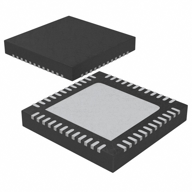
With a low input-to-output delay of typically less than 1.7ns and low skew between outputs within banks (<40ps), the PI6C49S1510ZDIE ensures precise clock distribution. It operates over an industrial temperature range of -40°C to 85°C and is available in a 48-TQFN (7x7) package, suitable for surface mounting.
Applications for this device include networking systems such as switches and routers, as well as high-frequency backplane-based computing and telecom platforms. Its ability to distribute low-jitter clock signals makes it ideal for demanding system designs.
| Qty | Low | High |
|---|---|---|
| 1+ | $4.44 | $4.44 |
Estimated market price range - modelled values for guidance only, not live distributor offers.
The maximum output frequency for differential outputs is 1.5 GHz, and for the LVCMOS reference output, it is 200 MHz.
The device supports user-configurable output signaling standards including LVDS, LVPECL, and HCSL for its differential outputs.
The typical additive phase jitter is less than 0.03 ps for the 12KHz to 20MHz integration range and less than 0.02 ps for the 10kHz to 1MHz integration range.
The operating voltage range is from 2.375V to 3.465V.
The operating temperature range is -40°C to 85°C.
The device is supplied in a 48-TQFN (7x7) package, which is a 48-VFQFN exposed pad type suitable for surface mounting.