

| Distributor | Stock | Pricing | MOQ | PKG | Lead Time | Date Code | On Order Quantity | On Order Delivery | |
|---|---|---|---|---|---|---|---|---|---|
|
3,000 pcs
|
3000 pcs | On Request | 1 | On Request | On Request | 16+ | On Request | On Request |
| Category | |
| Manufacturer Name | |
| Differential | |
| Frequency | |
| Input | |
| Input Type | |
| Mounting Type | |
| Number of Circuits | |
| Number of Outputs | |
| Operating Temperature | |
| Output | |
| Ratio | |
| Supplier Device Package | |
| Supplier Package | |
| Type | |
| Voltage |
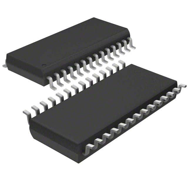
The PI6C49S1504LIEX from Diodes Incorporated is a high-performance fanout buffer designed for distributing low jitter clock signals. It supports output frequencies up to 1.5 GHz for its differential outputs and offers a LVCMOS reference output up to 200 MHz.
This device features 4 differential outputs organized in 2 banks, with user-configurable signaling standards for each bank, supporting LVDS, LVPECL, or HCSL. It accepts selectable reference inputs, including single-ended, differential, or crystal sources. The buffer boasts ultra-low additive phase jitter of less than 0.03 ps (typ) and low skew between outputs within banks (<40 ps).
Operating over an industrial temperature range of -40°C to 85°C, the PI6C49S1504LIEX is supplied in a 28-TSSOP package. It operates from a power supply voltage range of 2.375V to 3.465V, with separate input/output supply voltage for level shifting. This buffer is ideal for networking systems, high-frequency backplanes, computing, and telecom platforms requiring reliable clock distribution.
Key electrical characteristics include a low input-to-output delay (typ. < 1.5 ns) and support for 2.5V/3.3V power supplies. The device also includes proprietary input detection techniques to ensure illegal input conditions are reflected by output states.
| Qty | Low | High |
|---|---|---|
| 1+ | $4.44 | $4.44 |
Estimated market price range - modelled values for guidance only, not live distributor offers.
The PI6C49S1504LIEX supports an output frequency of up to 1.5 GHz for its differential outputs.
The outputs can be configured for LVDS, LVPECL, or HCSL signaling standards for each bank.
The operating temperature range for the PI6C49S1504LIEX is -40°C to 85°C.
This device is supplied in a 28-TSSOP package.
The typical additive phase jitter is less than 0.03 ps, measured with a differential signal at 156.25MHz over a 12KHz to 20MHz integration range.
The device operates from a power supply voltage range of 2.375V to 3.465V.