

| Distributor | Stock | Pricing | MOQ | PKG | Lead Time | Date Code | On Order Quantity | On Order Delivery | |
|---|---|---|---|---|---|---|---|---|---|
|
12,000 pcs
|
12000 pcs | On Request | 1 | On Request | On Request | On Request | On Request | On Request |
| Category | |
| Manufacturer Name | |
| Current | |
| Drain to Source Voltage (Vdss) | |
| Drive Voltage (Max Rds On, Min Rds On) | |
| FET Type | |
| Gate Charge (Qg) (Max) @ Vgs | |
| Input Capacitance (Ciss) (Max) @ Vds | |
| Lead Spacing | |
| Mounting Type | |
| Operating Temperature | |
| Power Dissipation (Max) | |
| Rds On (Max) @ Id, Vgs | |
| Supplier Device Package | |
| Technology | |
| Vgs (Max) | |
| Vgs(th) (Max) @ Id |
The NVTFWS040N10MCLTAG from ON Semiconductor is a single N-Channel MOSFET designed for power applications. It offers a drain-to-source voltage (Vds) of 100V and a maximum on-resistance (Rds(on)) of 38 mOhm at 5A and 10V gate-to-source voltage. The device can handle a continuous drain current of up to 21A at 25°C case temperature and 6.1A at 25°C ambient temperature.
Key electrical characteristics include a gate-to-source voltage (Vgs) range of ±20V and a gate threshold voltage (Vgs(th)) of 3V at 26µA. It has an input capacitance (Ciss) of 520 pF at 50V and a gate charge (Qg) of 8.6 nC at 10V.
This MOSFET is suitable for applications requiring low conduction and driver losses due to its low Rds(on) and low capacitance. It operates within a temperature range of -55°C to 175°C (TJ).
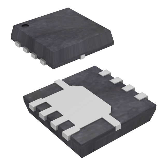
The NVTFWS040N10MCLTAG is available in a compact 8-WDFN (3.3x3.3 mm) surface mount package, making it ideal for space-constrained designs. It is AEC-Q101 qualified and PPAP capable, indicating its suitability for automotive applications. The device is also Pb-Free and RoHS Compliant.
| Qty | Low | High |
|---|---|---|
| 1+ | $0.33 | $0.33 |
Estimated market price range - modelled values for guidance only, not live distributor offers.
The drain-to-source voltage (Vds) is 100V.
The maximum on-resistance (Rds(on)) is 38 mOhm at 5A and 10V.
The continuous drain current is 21A at 25°C case temperature and 6.1A at 25°C ambient temperature.
The operating temperature range is -55°C to 175°C (TJ).
It is in an 8-PowerWDFN package, suitable for surface mounting.