

| Distributor | Stock | Pricing | MOQ | PKG | Lead Time | Date Code | On Order Quantity | On Order Delivery | |
|---|---|---|---|---|---|---|---|---|---|
|
23,930 pcs
|
23930 pcs | On Request | 1 | On Request | On Request | On Request | On Request | On Request |
| Category | |
| Manufacturer Name | |
| Current | |
| Drain to Source Voltage (Vdss) | |
| Drive Voltage (Max Rds On, Min Rds On) | |
| FET Type | |
| Gate Charge (Qg) (Max) @ Vgs | |
| Input Capacitance (Ciss) (Max) @ Vds | |
| Mounting Type | |
| Operating Temperature | |
| Power Dissipation (Max) | |
| Rds On (Max) @ Id, Vgs | |
| Supplier Device Package | |
| Tape & Reel | |
| Technology | |
| Vgs (Max) | |
| Vgs(th) (Max) @ Id |
The NVMYS8D0N04CTWG is a single N-Channel MOSFET designed for power applications. It features a drain-to-source voltage (Vdss) of 40V and a maximum continuous drain current of 49A at 25°C case temperature, with a lower rating of 16A at 25°C ambient temperature.
This MOSFET boasts a low on-resistance (Rds(on)) of 8.1mOhm at 15A and 10V gate drive, minimizing conduction losses. Its gate charge (Qg) is 10nC at 10V, and input capacitance (Ciss) is 625pF at 25V, contributing to reduced driver losses.
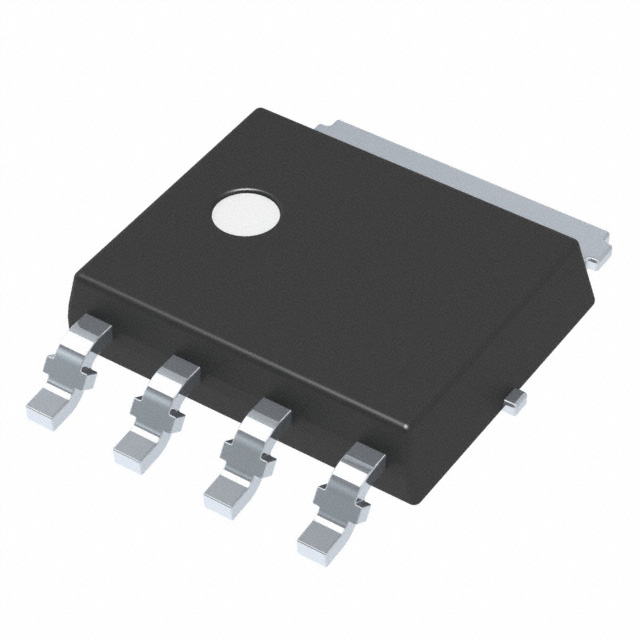
The device operates within a wide temperature range of -55°C to +175°C. It is housed in a compact LFPAK4 (5x6 mm) package, suitable for space-constrained designs. The MOSFET is AEC-Q101 qualified and PPAP capable, indicating its suitability for automotive and high-reliability applications.
Key electrical characteristics include a gate threshold voltage (Vgs(th)) of 3.5V maximum at 30µA. The maximum power dissipation is 38W at 25°C case temperature and 3.8W at 25°C ambient temperature. It is Pb-free and RoHS compliant.
| Qty | Low | High |
|---|---|---|
| 1+ | $0.99 | $0.99 |
Estimated market price range - modelled values for guidance only, not live distributor offers.
The drain-to-source voltage (Vdss) is 40V.
The maximum continuous drain current is 49A at 25°C case temperature and 16A at 25°C ambient temperature.
The Rds On is a maximum of 8.1mOhm at 15A drain current and 10V gate-source voltage.
The operating junction and storage temperature range is -55°C to +175°C.
The MOSFET is supplied in the LFPAK4 (5x6 mm) package.
Yes, the device is RoHS3 compliant.