

| Distributor | Stock | Pricing | MOQ | PKG | Lead Time | Date Code | On Order Quantity | On Order Delivery | |
|---|---|---|---|---|---|---|---|---|---|
|
20,000 pcs
|
20000 pcs | On Request | 1 | On Request | On Request | On Request | On Request | On Request |
| Category | |
| Manufacturer Name | |
| AEC Qualified | |
| Automotive Grade | |
| Configuration | |
| Current | |
| Drain to Source Voltage (Vdss) | |
| FET Feature | |
| Gate Charge (Qg) (Max) @ Vgs | |
| Industrial Grade | |
| Input Capacitance (Ciss) (Max) @ Vds | |
| Lead Spacing | |
| Medical Grade | |
| Military Grade | |
| Mounting Type | |
| Power | |
| Rds On (Max) @ Id, Vgs | |
| Storage Temperature | |
| Supplier Device Package | |
| Tape & Reel | |
| Technology | |
| Vgs(th) (Max) @ Id |
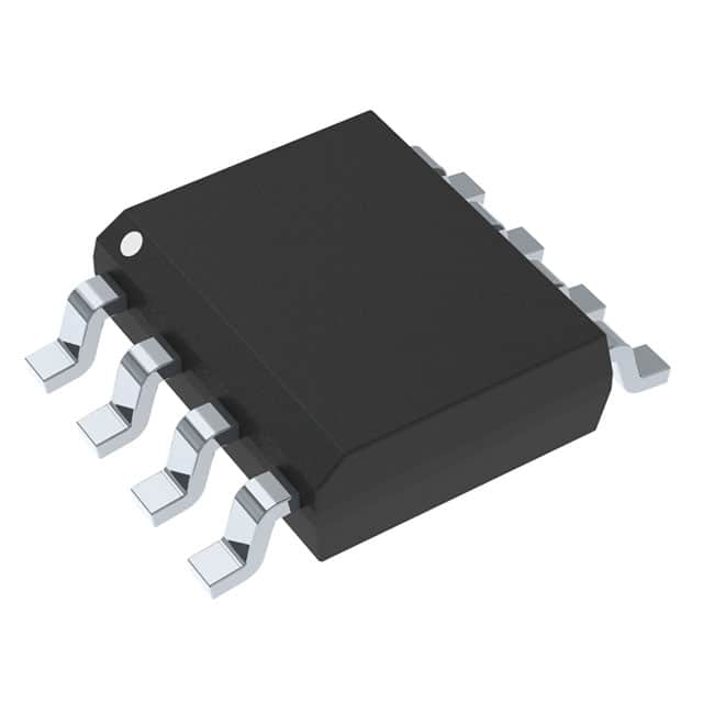
The NVMD6P02R2G is a Dual P-Channel MOSFET manufactured by On Semiconductor. This component is designed for surface mount applications and comes in an 8-SOIC package.
Key electrical specifications include a maximum drain-to-source voltage (Vdss) of 20V and a continuous drain current (ID) of 4.8A. The Rds On is specified at a maximum of 33mOhm at 6.2A and 4.5V. Input capacitance (Ciss) is 1700pF at 16V, and gate charge (Qg) is a maximum of 35nC at 4.5V. The gate threshold voltage (Vgs(th)) is a maximum of 1.2V at 250µA. The device has a maximum power dissipation of 750mW.
This MOSFET utilizes Metal Oxide Semiconductor technology and features a Logic Level Gate. Its configuration consists of two P-Channel MOSFETs in a dual arrangement. The component is suitable for various electronic designs requiring efficient switching and power management.
| Qty | Low | High |
|---|---|---|
| 1+ | $0.99 | $0.99 |
Estimated market price range - modelled values for guidance only, not live distributor offers.
The drain-to-source voltage (Vdss) for the NVMD6P02R2G is 20V.
The continuous drain current (ID) of the NVMD6P02R2G is 4.8A.
The Rds On (Max) for the NVMD6P02R2G is 33mOhm at 6.2A and 4.5V.
The NVMD6P02R2G comes in an 8-SOIC package.
The NVMD6P02R2G is RoHS3 Compliant.