

| Distributor | Stock | Pricing | MOQ | PKG | Lead Time | Date Code | On Order Quantity | On Order Delivery | |
|---|---|---|---|---|---|---|---|---|---|
|
94,800 pcs
|
94800 pcs | On Request | 1 | On Request | On Request | 1651+ | On Request | On Request |
| Category | |
| Manufacturer Name | |
| Current | |
| Drain to Source Voltage (Vdss) | |
| Drive Voltage (Max Rds On, Min Rds On) | |
| FET Type | |
| Gate Charge (Qg) (Max) @ Vgs | |
| Halogen Free | |
| Input Capacitance (Ciss) (Max) @ Vds | |
| Mounting Type | |
| Operating Temperature | |
| Power Dissipation (Max) | |
| Rds On (Max) @ Id, Vgs | |
| Storage Temperature | |
| Supplier Device Package | |
| Tape & Reel | |
| Technology | |
| Vgs (Max) | |
| Vgs(th) (Max) @ Id |
The NVJS4151PT1G from ON Semiconductor is a P-Channel MOSFET designed for power applications. It features leading Trench technology for low RDS(ON), contributing to extended battery life. The device has a drain-to-source voltage of -20V and a continuous drain current of -3.2A at 25°C ambient temperature.
Key electrical characteristics include a maximum Rds On of 67mOhm at 2.9A and 4.5V, and a gate threshold voltage of 1.2V maximum at 250µA. The MOSFET is rated for a maximum power dissipation of 1.2W at 25°C.
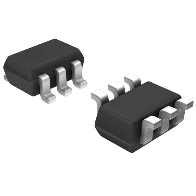
This component is housed in an SC-88 (SOT-363) small outline package, measuring 2x2 mm, designed for maximum circuit board utilization. It includes gate diodes for ESD protection and is AEC-Q101 qualified and PPAP capable. The device is Pb-Free, Halogen Free/BFR Free, and RoHS Compliant.
Applications for the NVJS4151PT1G include high-side load switching in devices such as cell phones, computing equipment, digital cameras, MP3 players, and PDAs.
| Qty | Low | High |
|---|---|---|
| 1+ | $0.99 | $0.99 |
Estimated market price range - modelled values for guidance only, not live distributor offers.
-20 V
-3.2 A (Ta)
67mOhm @ 2.9A, 4.5V
SC-88
-55°C ~ 150°C (TJ)
RoHS3 Compliant