

| Category | |
| Manufacturer Name | |
| Current | |
| Drain to Source Voltage (Vdss) | |
| Drive Voltage (Max Rds On, Min Rds On) | |
| FET Type | |
| Gate Charge (Qg) (Max) @ Vgs | |
| Input Capacitance (Ciss) (Max) @ Vds | |
| Mounting Type | |
| Operating Temperature | |
| Power Dissipation (Max) | |
| Rds On (Max) @ Id, Vgs | |
| Supplier Device Package | |
| Tape & Reel | |
| Technology | |
| Vgs (Max) | |
| Vgs(th) (Max) @ Id |
The ON Semiconductor NTR2101PT1G is a P-Channel, small-signal MOSFET designed for various applications including high-side load switching and DC-DC conversion. It utilizes leading trench technology for low on-resistance (RDS(on)).
Key electrical characteristics include a drain-to-source voltage (Vdss) of -8.0 V and a continuous drain current of -3.7 A at 25°C. The gate-source voltage (Vgs) range is ±8.0 V, with a gate threshold voltage (Vgs(th)) of 1V at 250µA. The device offers low RDS(on) values, such as 52mOhm at 3.5A and 4.5V Vgs.
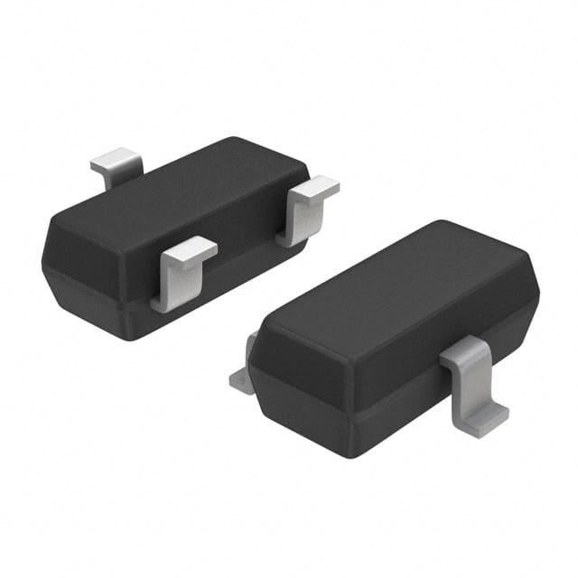
This MOSFET is packaged in a SOT-23 surface-mount package, making it suitable for applications where space is limited, such as cell phones, notebooks, and PDAs. The operating temperature range is -55°C to 150°C.
The NTR2101PT1G is a Pb-Free device, aligning with environmental standards.
| Qty | Low | High |
|---|---|---|
| 1+ | $0.99 | $0.99 |
Estimated market price range - modelled values for guidance only, not live distributor offers.
The drain-to-source voltage (Vdss) is -8.0 V.
The continuous drain current is -3.7 A at 25°C.
The RDS(on) is 52mOhm at a drain current of 3.5A and gate-source voltage of 4.5V.
The operating junction and storage temperature range is -55°C to 150°C.
It is supplied in a SOT-23-3 (TO-236) surface-mount package.
Yes, the NTR2101PT1G is RoHS3 Compliant.
The Moisture Sensitivity Level is 1.