

| Distributor | Stock | Pricing | MOQ | PKG | Lead Time | Date Code | On Order Quantity | On Order Delivery | |
|---|---|---|---|---|---|---|---|---|---|
|
27,000 pcs
|
27000 pcs | On Request | 1 | On Request | On Request | On Request | On Request | On Request |
| Category | |
| Manufacturer Name | |
| Current | |
| Drain to Source Voltage (Vdss) | |
| Drive Voltage (Max Rds On, Min Rds On) | |
| FET Feature | |
| FET Type | |
| Gate Charge (Qg) (Max) @ Vgs | |
| Input Capacitance (Ciss) (Max) @ Vds | |
| Lead Spacing | |
| Mounting Type | |
| Operating Temperature | |
| Power Dissipation (Max) | |
| Rds On (Max) @ Id, Vgs | |
| Supplier Device Package | |
| Supplier Package | |
| Tape & Reel | |
| Technology | |
| Vgs (Max) | |
| Vgs(th) (Max) @ Id |
The ON Semiconductor NTLJF3117PT1G is a P-Channel MOSFET designed for various electronic applications. It features a maximum drain-source voltage (Vds) of 20V and a continuous drain current (Id) of 2.3A at ambient temperature. The MOSFET offers a low on-resistance (Rds On) of 100mOhm at 2A and 4.5Vgs, with a gate threshold voltage (Vgs(th)) of 1V at 250µA.
This device operates within a temperature range of -55°C to 150°C (TJ) and has a power dissipation of 710mW (Ta). Key electrical characteristics include an input capacitance (Ciss) of 531pF at 10Vds and a gate charge (Qg) of 6.2nC at 4.5Vgs. It also incorporates a Schottky Diode feature.
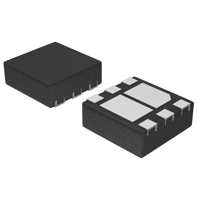
The NTLJF3117PT1G is packaged in a 6-WDFN Exposed Pad (2x2) and is designed for surface mounting. Its technology is based on MOSFET (Metal Oxide) principles. The RoHS status is compliant, and it has an MSL rating of 1.
| Qty | Low | High |
|---|---|---|
| 1+ | $0.99 | $0.99 |
Estimated market price range - modelled values for guidance only, not live distributor offers.
The drain-source voltage (Vdss) for the NTLJF3117PT1G is 20V.
The continuous drain current (Id) for the NTLJF3117PT1G is 2.3A at ambient temperature.
The maximum Rds On for the NTLJF3117PT1G is 100mOhm at 2A and 4.5Vgs.
The operating temperature range for the NTLJF3117PT1G is -55°C to 150°C (TJ).
The NTLJF3117PT1G is in a 6-WDFN Exposed Pad package, designed for surface mounting.
Yes, the NTLJF3117PT1G is RoHS3 Compliant.
The Moisture Sensitivity Level (MSL) for the NTLJF3117PT1G is 1 Unlimited.