

| Distributor | Stock | Pricing | MOQ | PKG | Lead Time | Date Code | On Order Quantity | On Order Delivery | |
|---|---|---|---|---|---|---|---|---|---|
|
22,020 pcs
|
22020 pcs | On Request | 1 | On Request | On Request | On Request | On Request | On Request | |
|
22,020 pcs
|
22020 pcs | On Request | 1 | On Request | On Request | On Request | On Request | On Request | |
|
1,619 pcs
|
1619 pcs | On Request | 1 | On Request | On Request | On Request | On Request | On Request |
| Category | |
| Manufacturer Name | |
| Configuration | |
| Current | |
| Drain to Source Voltage (Vdss) | |
| FET Feature | |
| Gate Charge (Qg) (Max) @ Vgs | |
| Input Capacitance (Ciss) (Max) @ Vds | |
| Lead Spacing | |
| Mounting Type | |
| Operating Temperature | |
| Power | |
| Rds On (Max) @ Id, Vgs | |
| Supplier Device Package | |
| Tape & Reel | |
| Technology | |
| Vgs(th) (Max) @ Id |
The ON Semiconductor NTLJD3119CTBG is a complementary power MOSFET featuring both N-channel and P-channel transistors within a single package. This device is designed for applications requiring efficient power management, such as synchronous DC-DC conversion circuits and load/power management in portable devices.
Key electrical characteristics include a drain-source voltage of 20V for the N-channel and -20V for the P-channel. The N-channel offers a continuous drain current of 3.8A (steady state at 25°C) with a low on-resistance of 65mOhm at 3.8A and 4.5V Vgs. The P-channel provides a continuous drain current of -3.3A (steady state at 25°C).
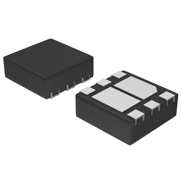
This MOSFET utilizes leading-edge trench technology for low on-resistance and is housed in a compact 6-WDFN package with an exposed drain pad for excellent thermal conduction. The low profile (<0.8 mm) makes it suitable for thin environments. It operates over a wide temperature range of -55°C to 150°C.
Applications include synchronous DC-DC conversion, load/power management in PDAs, cellular phones, and hard drives, as well as color display and camera flash regulators.
| Qty | Low | High |
|---|---|---|
| 1+ | $0.99 | $0.99 |
Estimated market price range - modelled values for guidance only, not live distributor offers.
The drain-source breakdown voltage is 20V for the N-channel and -20V for the P-channel.
The N-channel continuous drain current is 3.8A (steady state at 25°C), and the P-channel continuous drain current is -3.3A (steady state at 25°C).
The Rds On resistance for the N-channel is a maximum of 65mOhm at 3.8A and 4.5V Vgs.
The operating temperature range is -55°C to 150°C (TJ).
It is supplied in a 6-WDFN Exposed Pad package, measuring 2x2mm.
Yes, this device is RoHS3 Compliant.