

| Distributor | Stock | Pricing | MOQ | PKG | Lead Time | Date Code | On Order Quantity | On Order Delivery | |
|---|---|---|---|---|---|---|---|---|---|
|
2,206 pcs
|
2206 pcs | On Request | 1 | On Request | On Request | 0951+ | On Request | On Request |
| Category | |
| Manufacturer Name | |
| Configuration | |
| Current | |
| Drain to Source Voltage (Vdss) | |
| FET Feature | |
| Gate Charge (Qg) (Max) @ Vgs | |
| Input Capacitance (Ciss) (Max) @ Vds | |
| Lead Spacing | |
| Mounting Type | |
| Operating Temperature | |
| Power | |
| Rds On (Max) @ Id, Vgs | |
| Supplier Device Package | |
| Tape & Reel | |
| Technology | |
| Vgs(th) (Max) @ Id |
The NTLJD3119CTAG is a complementary N-Channel and P-Channel MOSFET designed by ON Semiconductor. This device offers a drain-source voltage of 20V for the N-channel and -20V for the P-channel. It supports continuous drain currents up to 4.6A (N-Ch) and -4.1A (P-Ch) under pulsed conditions.
Key electrical characteristics include a low on-resistance of 65mOhm at 3.8A and 4.5V Vgs, and a gate threshold voltage of 1V maximum at 250µA. The MOSFET utilizes leading-edge trench technology for low on-resistance and features a logic-level gate.
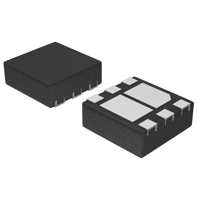
Packaged in a compact 6-WDFN (2x2 mm) with an exposed drain pad for excellent thermal conduction, the NTLJD3119CTAG is suitable for applications requiring efficient power management. Its low profile makes it ideal for thin environments.
Applications include synchronous DC-DC conversion circuits, load/power management of portable devices like PDAs and cellular phones, and color display and camera flash regulators.
| Qty | Low | High |
|---|---|---|
| 1+ | $0.99 | $0.99 |
Estimated market price range - modelled values for guidance only, not live distributor offers.
The drain-source voltage is 20V for the N-Channel and -20V for the P-Channel.
The maximum continuous drain current is 3.8A for N-Channel and -3.3A for P-Channel at 25°C.
The Rds On is a maximum of 65mOhm at 3.8A and 4.5V Vgs.
The operating junction and storage temperature range is -55°C to 150°C.
It is in a 6-WDFN Exposed Pad package, measuring 2x2mm.
Yes, it is RoHS3 Compliant.