

| Distributor | Stock | Pricing | MOQ | PKG | Lead Time | Date Code | On Order Quantity | On Order Delivery | |
|---|---|---|---|---|---|---|---|---|---|
|
1,040 pcs
|
1040 pcs | On Request | 1 | On Request | On Request | 0412+ | On Request | On Request |
| Category | |
| Manufacturer Name | |
| Configuration | |
| Continuous Drain Current (Typical @ TA = 25 °C) | |
| Continuous Drain Current (Typical @ TA = 85 °C) | |
| Current | |
| Drain To Source Breakdown Voltage (Minimum @ N-Ch, VGS = 0 V, ID = 250 µA) | |
| Drain To Source Breakdown Voltage (Minimum @ P-Ch, ID = -250 µA) | |
| Drain to Source Voltage (Vdss) | |
| FET Feature | |
| Gate Charge (Qg) (Max) @ Vgs | |
| Gate to Source Voltage (Vgs) | |
| Input Capacitance (Ciss) (Max) @ Vds | |
| Junction To Ambient Thermal Resistance (Typical/Maximum @ Steady State (Based on R/C 0113 JA) | |
| Junction To Lead Thermal Resistance (Typical/Maximum @ Steady State (Based on R/C 0113 JL) | |
| Mounting Type | |
| Operating Temperature | |
| Power | |
| Power Dissipation (Typical @ TA = 25 °C (Based on R/C 0113 JA) | |
| Power Dissipation (Typical @ TA = 25 °C (Based on R/C 0113 JL) | |
| Power Dissipation (Typical @ TA = 85 °C (Based on R/C 0113 JA) | |
| Power Dissipation (Typical @ TA = 85 °C (Based on R/C 0113 JL) | |
| Pulsed Drain Current (Idm) | |
| Rds On (Max) @ Id, Vgs | |
| Rds On Max (Typical @ N-Ch @ 2.5 V) | |
| Rds On Max (Typical @ N-Ch @ 4.5 V) | |
| Rds On Max (Typical @ P-Ch @ -1.8 V) | |
| Rds On Max (Typical @ P-Ch @ -2.5 V) | |
| Rds On Max (Typical @ P-Ch @ -4.5 V) | |
| Supplier Device Package | |
| Supplier Package | |
| Technology | |
| Vgs(th) (Max) @ Id |
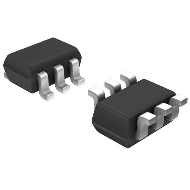
The NTJD4105CT2 from On Semiconductor is a complementary MOSFET array featuring both N-channel and P-channel devices within a single SC-88 package. This configuration is suitable for applications requiring space-saving solutions.
The device offers a drain-to-source voltage rating of 20V for the N-channel and -8.0V for the P-channel. Continuous drain current capabilities are 630mA for the N-channel and -775mA for the P-channel at 25°C. The Rds On is specified at a typical 375mOhm at 630mA and 4.5V gate-source voltage for the N-channel.
With a low threshold voltage of 1.5V and logic-level gate feature, this MOSFET array is designed for efficient switching. It operates across a wide temperature range of -55°C to 150°C.
The SC-88 package provides a small footprint, making it ideal for portable electronics and space-constrained designs. Applications include DC-DC conversion, load switching, and power management in battery-supplied devices like cell phones and digital cameras.
| Qty | Low | High |
|---|---|---|
| 1+ | $0.99 | $0.99 |
Estimated market price range - modelled values for guidance only, not live distributor offers.
The drain-to-source voltage is 20V for the N-channel and -8.0V for the P-channel.
The continuous drain current is 630mA for the N-channel and -775mA for the P-channel at 25°C.
The typical Rds On is 375mOhm at 630mA and 4.5V gate-source voltage for the N-channel.
The operating junction and storage temperature range is -55°C to 150°C.
The NTJD4105CT2 is supplied in an SC-88/SC70-6/SOT-363 package.
Yes, the NTJD4105CT2 is RoHS3 Compliant.