

| Distributor | Stock | Pricing | MOQ | PKG | Lead Time | Date Code | On Order Quantity | On Order Delivery | |
|---|---|---|---|---|---|---|---|---|---|
|
64,020 pcs
|
64020 pcs | On Request | 1 | On Request | On Request | On Request | On Request | On Request | |
|
5,799 pcs
|
5799 pcs | On Request | 1 | On Request | On Request | On Request | On Request | On Request | |
|
5,470 pcs
|
5470 pcs | On Request | 1 | On Request | On Request | 24+ | On Request | On Request | |
|
2,348 pcs
|
2348 pcs | On Request | 1 | On Request | On Request | On Request | On Request | On Request | |
|
1,591 pcs
|
1591 pcs | On Request | 1 | On Request | On Request | 0831+ | On Request | On Request | |
|
500 pcs
|
500 pcs | On Request | 1 | On Request | On Request | On Request | On Request | On Request |
| Category | |
| Manufacturer Name | |
| Configuration | |
| Current | |
| Drain to Source Voltage (Vdss) | |
| FET Feature | |
| Gate Charge (Qg) (Max) @ Vgs | |
| Input Capacitance (Ciss) (Max) @ Vds | |
| Mounting Type | |
| Operating Temperature | |
| Power | |
| Rds On (Max) @ Id, Vgs | |
| Supplier Device Package | |
| Supplier Package | |
| Technology | |
| Vgs(th) (Max) @ Id |
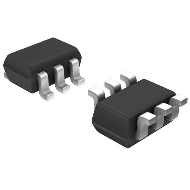
The NTJD4105CT1G from ON Semiconductor is a complementary MOSFET featuring both N-channel and P-channel devices within a single SC-88 package. This configuration is suitable for applications requiring space-saving solutions.
Key electrical characteristics include a drain-to-source voltage of 20V for the N-channel and -8.0V for the P-channel. The continuous drain current is rated at 630mA for the N-channel and -775mA for the P-channel at 25°C. The on-resistance (RDS(on)) is specified as 375mOhm at 630mA and 4.5V gate-source voltage.
This MOSFET is designed for applications such as DC-DC conversion, load/power switching, and is suitable for use in single or dual cell Li-Ion battery-supplied devices like cell phones, MP3 players, digital cameras, and PDAs. The device operates over a temperature range of -55°C to 150°C.
The component is housed in an SC-88/SC70-6/SOT-363 package, designed for surface mounting. It offers ESD protection on the gate and is available in Pb-Free packages.
| Qty | Low | High |
|---|---|---|
| 1+ | $0.99 | $0.99 |
Estimated market price range - modelled values for guidance only, not live distributor offers.
The drain-to-source voltage is 20V for the N-channel and -8.0V for the P-channel.
The continuous drain current is 630mA for the N-channel and -775mA for the P-channel at 25°C.
The on-resistance is a maximum of 375mOhm at 630mA and 4.5V gate-source voltage.
The operating junction and storage temperature range is -55°C to 150°C.
The NTJD4105CT1G is supplied in an SC-88/SC70-6/SOT-363 package.