

| Category | |
| Manufacturer Name | |
| Configuration | |
| Current | |
| Drain to Source Voltage (Vdss) | |
| Gate Charge (Qg) (Max) @ Vgs | |
| Input Capacitance (Ciss) (Max) @ Vds | |
| Mounting Type | |
| Operating Temperature | |
| Power | |
| Rds On (Max) @ Id, Vgs | |
| Supplier Device Package | |
| Tape & Reel | |
| Technology | |
| Vgs(th) (Max) @ Id |
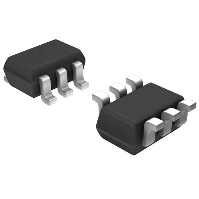
The ON Semiconductor NTJD4001NT1G is a dual, N-channel, small-signal MOSFET housed in a compact SC-88/SC70-6/SOT-363 package. This device offers a drain-to-source voltage (Vdss) of 30V and a continuous drain current (Id) of 250mA at 25°C. It is designed for applications requiring low gate charge for fast switching and a small footprint, being 30% smaller than TSOP-6 packages.
Key electrical characteristics include a maximum gate threshold voltage (Vgs(th)) of 1.5V at 100µA and a maximum on-resistance (Rds On) of 1.5 Ohm at 10mA and 4V. The device also features ESD protected gates and is AEC Q101 qualified for the NVTJD4001N variant.
This MOSFET is suitable for low-side load switching, Li-Ion battery supplied devices such as cell phones and PDAs, buck converters, and level shifting applications. It is RoHS compliant and available in tape and reel packaging for automated assembly.
| Qty | Low | High |
|---|---|---|
| 1+ | $0.99 | $0.99 |
Estimated market price range - modelled values for guidance only, not live distributor offers.
The drain-to-source voltage (Vdss) of the NTJD4001NT1G is 30V.
The continuous drain current (Id) is 250mA at 25°C and 180mA at 85°C.
The NTJD4001NT1G is available in the SC-88/SC70-6/SOT-363 package.
The operating temperature range is -55°C to 150°C (TJ).
Yes, the NTJD4001NT1G is RoHS3 Compliant.