

| Distributor | Stock | Pricing | MOQ | PKG | Lead Time | Date Code | On Order Quantity | On Order Delivery | |
|---|---|---|---|---|---|---|---|---|---|
|
1,470 pcs
|
1470 pcs | On Request | 1 | On Request | On Request | On Request | On Request | On Request | |
|
1,000 pcs
|
1000 pcs | On Request | 1 | On Request | On Request | On Request | On Request | On Request |
| Category | |
| Manufacturer Name | |
| Current | |
| Drain to Source Voltage (Vdss) | |
| Drive Voltage (Max Rds On, Min Rds On) | |
| FET Type | |
| Gate Charge (Qg) (Max) @ Vgs | |
| Input Capacitance (Ciss) (Max) @ Vds | |
| Mounting Type | |
| Operating Temperature | |
| Power Dissipation (Max) | |
| Rds On (Max) @ Id, Vgs | |
| Supplier Device Package | |
| Supplier Package | |
| Technology | |
| Vgs (Max) | |
| Vgs(th) (Max) @ Id |
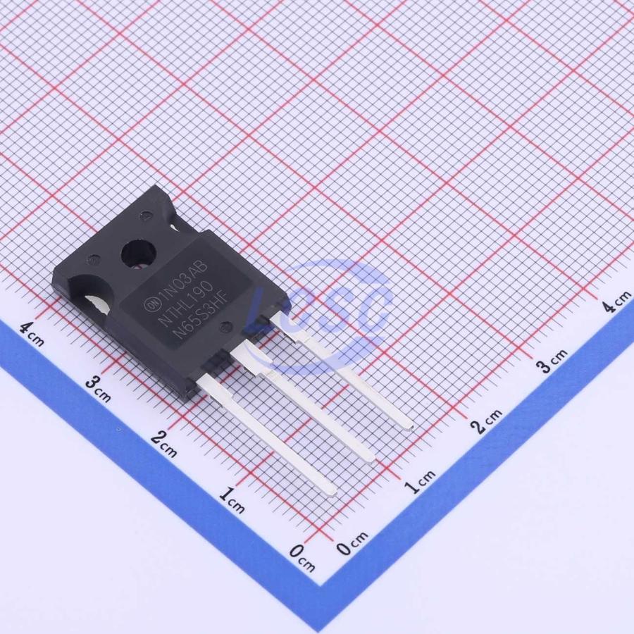
The NTHL190N65S3HF from On Semiconductor is a high-performance N-Channel MOSFET belonging to the SUPERFET III family. This device leverages advanced charge balance technology to achieve outstanding low on-resistance and reduced gate charge, making it suitable for applications demanding high efficiency and minimized conduction losses.
Key electrical characteristics include a Drain to Source Voltage (Vdss) of 650V, a continuous Drain Current (ID) of 20A at 25°C, and a maximum On-Resistance (Rds On) of 190mOhm at 10A and 10V. The typical Gate Charge (Qg) is 34 nC, and the typical Effective Output Capacitance (Coss(eff.)) is 316 pF.
This MOSFET is designed to withstand extreme dv/dt rates and offers optimized reverse recovery performance of its body diode, potentially reducing the need for additional components and enhancing system reliability. It is packaged in a TO-247-3 lead package and is suitable for through-hole mounting.
Applications for the NTHL190N65S3HF include Telecom/Server Power Supplies, Industrial Power Supplies, EV Chargers, and UPS/Solar systems, where miniaturization and higher efficiency are critical.
| Qty | Low | High |
|---|---|---|
| 1+ | $3.04 | $3.04 |
Estimated market price range - modelled values for guidance only, not live distributor offers.
The maximum Drain to Source Voltage (Vdss) is 650 V.
The typical On-Resistance (Rds On) is 165 mOhm at 10V.
The typical Gate Charge (Qg) is 34 nC at 10V.
The operating temperature range is -55°C to 150°C (TJ).
The NTHL190N65S3HF is supplied in a TO-247-3 package.