

| Distributor | Stock | Pricing | MOQ | PKG | Lead Time | Date Code | On Order Quantity | On Order Delivery | |
|---|---|---|---|---|---|---|---|---|---|
|
2,870 pcs
|
2870 pcs | On Request | 1 | On Request | On Request | On Request | On Request | On Request |
| Category | |
| Manufacturer Name | |
| Current | |
| Current Drain (Id) | |
| Drain to Source Voltage (Vdss) | |
| FET Type | |
| Input Capacitance (Ciss) (Max) @ Vds | |
| Lead Style | |
| Mounting Type | |
| Operating Temperature | |
| Power | |
| Resistance | |
| Supplier Device Package | |
| Supplier Package | |
| Voltage |
The NSVJ6904DSB6T1G is a dual N-channel JFET manufactured by ON Semiconductor. This device is designed for compact size and high gain performance, making it suitable for applications such as AM tuner RF amplification and low noise amplifiers.
Key electrical specifications include a drain-to-source voltage of 25V, a maximum drain current of 50mA, and a typical forward transconductance of 40mS. The input capacitance (Ciss) is 6pF at 5V, and the noise figure is rated at 2.1dB to 2.8dB at 100MHz.
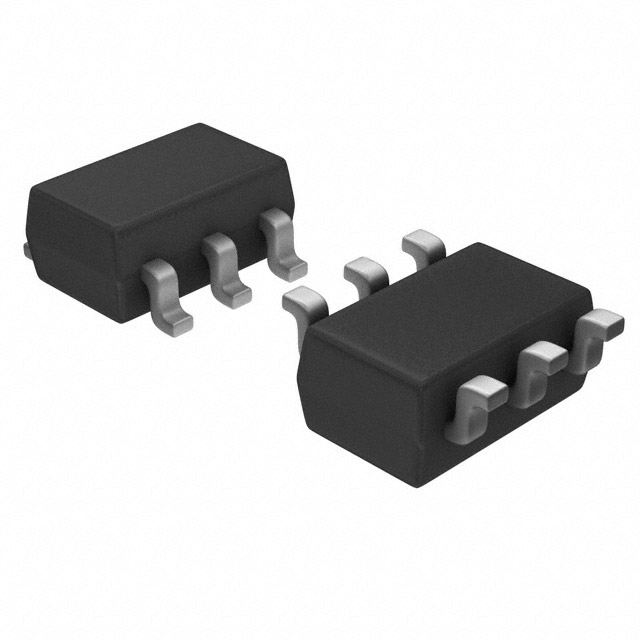
This JFET features a CPH6 package, which is pin-compatible with the SC-74 package. It is designed for surface mounting and operates within a temperature range of -55°C to +150°C. The device is AEC-Q101 qualified and PPAP capable, indicating its suitability for automotive applications.
| Qty | Low | High |
|---|---|---|
| 1+ | $0.99 | $0.99 |
Estimated market price range - modelled values for guidance only, not live distributor offers.
The drain-to-source voltage (Vdsx) is 25V.
The typical forward transconductance (|yfs|) is 40mS.
The operating junction and storage temperature range is -55°C to +150°C.
The NSVJ6904DSB6T1G is supplied in a CPH6 package.
The RoHS status is Compliant.
The input capacitance (Ciss) is 6pF at 5V.
Typical applications include AM tuner RF amplification and low noise amplifier circuits.