

| Distributor | Stock | Pricing | MOQ | PKG | Lead Time | Date Code | On Order Quantity | On Order Delivery | |
|---|---|---|---|---|---|---|---|---|---|
|
120,000 pcs
|
120000 pcs | On Request | 1 | On Request | On Request | On Request | On Request | On Request |
| Category | |
| Manufacturer Name | |
| AEC Qualified | |
| Automotive Grade | |
| Capacitance | |
| Capacitance @ Vr, F | |
| Current | |
| Diode Type | |
| Forward Voltage | |
| Halogen Free | |
| Industrial Grade | |
| Lead Style | |
| Medical Grade | |
| Military Grade | |
| Mounting Type | |
| Operating Temperature | |
| Resistance @ If, F | |
| Reverse Current | |
| SVHC Present | |
| Storage Temperature | |
| Supplier Device Package | |
| Tape & Reel | |
| Voltage |
The NSDP301MX2WT5G is a single PIN diode manufactured by onsemi (formerly On Semiconductor), designed for use in RF attenuator and switch circuits. This PIN diode offers low series resistance (1.3 Ohm typical at 10mA, 100MHz) and small interterminal capacitance (0.33 pF typical at 0V, 1MHz), making it suitable for high-frequency applications.
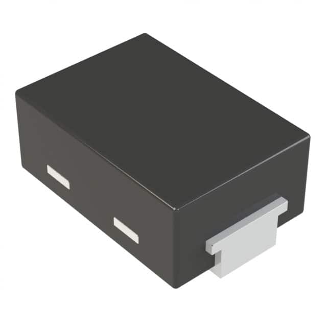
The device is housed in a compact X2DFNW2 package (2-XDFN, 2-X2DFNW (1x0.6)) with wettable flanks, which improves solder joint quality and inspection on PCB. It supports a maximum reverse voltage of 80V and forward current of 100mA, with a forward voltage range of 0.78V to 0.81V at 1mA. The operating junction temperature range is -55°C to 150°C.
The NSDP301MX2WT5G is RoHS compliant, Pb-Free, and Halogen Free. It is available in tape and reel packaging with a standard quantity of 8000 pieces per reel. An automotive-qualified variant (AEC-Q101) is also available under part number NSVDP301MX2WT5G.
| Qty | Low | High |
|---|---|---|
| 1+ | $0.65 | $0.65 |
| 10+ | $0.40 | $0.40 |
| 100+ | $0.25 | $0.25 |
| 500+ | $0.19 | $0.19 |
| 8,000+ | $0.19 | $0.19 |
Estimated market price range - modelled values for guidance only, not live distributor offers.
The maximum reverse voltage is 80V.
The maximum forward current is 100 mA.
The forward voltage ranges from 0.78 V to 0.81 V at 1 mA.
The device is housed in a 2-XDFN package (X2DFNW2, 2-X2DFNW (1x0.6)).
The typical series resistance is 1.3 Ohm at 10 mA and 100 MHz.
The typical capacitance is 0.33 pF at 0 V and 1 MHz.
The operating junction temperature range is -55°C to 150°C.