

| Distributor | Stock | Pricing | MOQ | PKG | Lead Time | Date Code | On Order Quantity | On Order Delivery | |
|---|---|---|---|---|---|---|---|---|---|
|
21,000 pcs
|
21000 pcs | On Request | 1 | On Request | On Request | On Request | On Request | On Request |
| Category | |
| Manufacturer Name | |
| Current | |
| Input Type | |
| Logic Type | |
| Mounting Type | |
| Number of Bits per Element | |
| Number of Elements | |
| Operating Temperature | |
| Output Type | |
| Supplier Device Package | |
| Supplier Package | |
| Voltage |
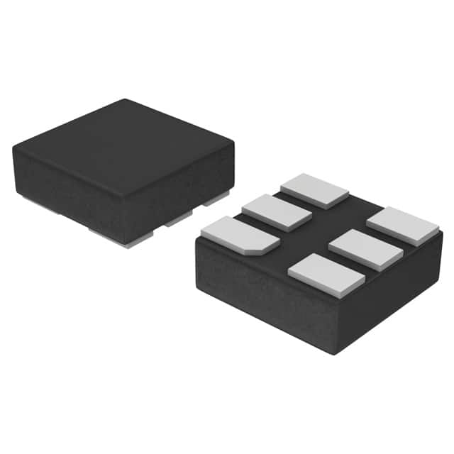
This dual Schmitt-trigger buffer, part number NLX2G17AMX1TCG from ON Semiconductor, is designed for high-speed CMOS applications. It offers a wide operating supply voltage range from 1.65V to 5.5V, making it versatile for various power systems. The device features non-inverting logic with Schmitt trigger inputs, enhancing noise immunity and waveform shaping capabilities.
Key electrical characteristics include an output current of 32mA for both source and sink, and a typical propagation delay of 3.1 ns at 5.0V. The operating temperature range is from -55°C to 125°C (TA), suitable for demanding environments. The NLX2G17AMX1TCG is available in a compact 6-ULLGA (1.45x1) package, designed for surface mounting.
This buffer is ideal for applications requiring reliable signal conditioning, noise reduction, or squaring up slow-changing waveforms. Its advanced CMOS technology ensures low power dissipation while maintaining high-speed performance. The ultra-small footprint of the 6-ULLGA package makes it suitable for space-constrained designs.
| Qty | Low | High |
|---|---|---|
| 1+ | $1.20 | $1.20 |
Estimated market price range - modelled values for guidance only, not live distributor offers.
The supply voltage range for the NLX2G17AMX1TCG is 1.65 V to 5.5 V.
The NLX2G17AMX1TCG operates within a temperature range of -55°C to 125°C.
The NLX2G17AMX1TCG is available in a 6-ULLGA or 6-XFLGA package.
The NLX2G17AMX1TCG has a Push-Pull output type.
The NLX2G17AMX1TCG has 2 elements.
The typical propagation delay is 3.1 ns when VCC is 5.0 V.