

| Distributor | Stock | Pricing | MOQ | PKG | Lead Time | Date Code | On Order Quantity | On Order Delivery | |
|---|---|---|---|---|---|---|---|---|---|
|
3,135 pcs
|
3135 pcs | On Request | 1 | On Request | On Request | On Request | On Request | On Request |
| Category | |
| Manufacturer Name | |
| Current | |
| Logic Type | |
| Max Propagation Delay @ V, Max CL | |
| Mounting Type | |
| Number of Circuits | |
| Number of Inputs | |
| Operating Temperature | |
| Output Current | |
| Supplier Device Package | |
| Supplier Package | |
| Voltage |
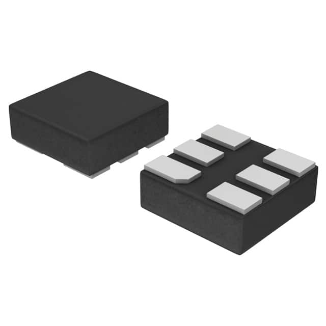
This NLX2G04BMX1TCG is a dual inverter IC manufactured by ON Semiconductor. It is designed for high-speed CMOS applications and comes in an ultra-small footprint.
The device supports a wide operating supply voltage range from 1.65V to 5.5V. It offers a maximum propagation delay of 3.6ns at 5V with a 50pF load capacitance, and a typical propagation delay of 1.8ns at 5V. The low power dissipation is indicated by a maximum supply current of 1µA at 25°C.
Input and output pins provide protection for voltages up to 7.0V, regardless of the supply voltage. The NLX2G04BMX1TCG features power-down protection on its inputs and balanced propagation delays. It is available in a compact 6-ULLGA surface mount package.
Key electrical characteristics include a maximum supply current of 100mA per supply pin and a maximum output current of 50mA. The operating temperature range is from -55°C to 125°C.
| Qty | Low | High |
|---|---|---|
| 1+ | $0.22 | $0.22 |
Estimated market price range - modelled values for guidance only, not live distributor offers.
The operating voltage range for the NLX2G04BMX1TCG is 1.65V to 5.5V.
The maximum propagation delay for the NLX2G04BMX1TCG is 3.6ns at 5V with a 50pF load.
The operating temperature range for the NLX2G04BMX1TCG is -55°C to 125°C.
The NLX2G04BMX1TCG is supplied in a 6-ULLGA package.
The NLX2G04BMX1TCG is RoHS3 compliant.
The Moisture Sensitivity Level (MSL) for the NLX2G04BMX1TCG is 1.