

| Distributor | Stock | Pricing | MOQ | PKG | Lead Time | Date Code | On Order Quantity | On Order Delivery | |
|---|---|---|---|---|---|---|---|---|---|
|
3,000 pcs
|
3000 pcs | On Request | 1 | On Request | On Request | On Request | On Request | On Request |
| Category | |
| Manufacturer Name | |
| Current | |
| Logic Type | |
| Max Propagation Delay @ V, Max CL | |
| Mounting Type | |
| Number of Circuits | |
| Number of Inputs | |
| Operating Temperature | |
| Power Dissipation | |
| Supplier Device Package | |
| Supplier Package | |
| Voltage |
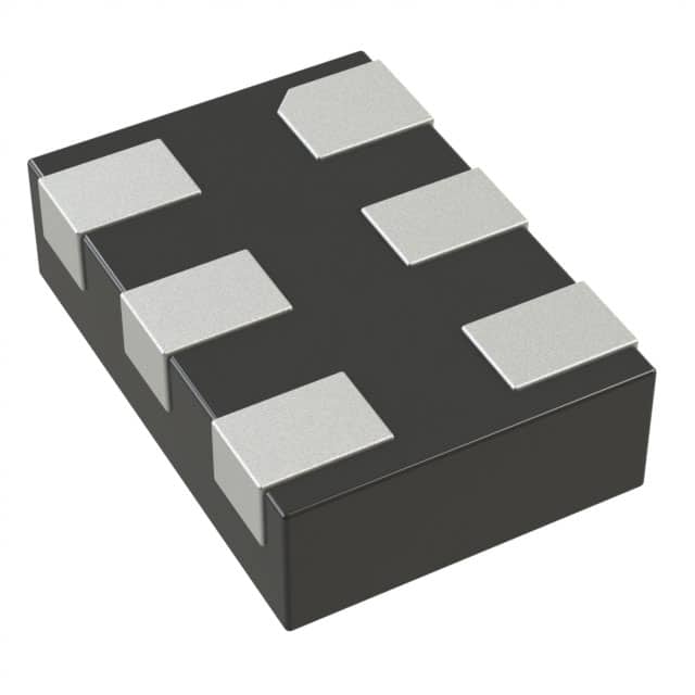
The NLX1G11AMUTCG from On Semiconductor is an advanced, high-speed 3-input CMOS AND gate packaged in an ultra-small UDFN footprint. This device is designed for versatile operation across a wide supply voltage range, from 1.65V to 5.5V.
Key electrical characteristics include a typical propagation delay of 2.4 ns at 5.0V. The gate features overvoltage tolerant input pins, providing protection when voltages up to 7.0V are applied, regardless of the supply voltage. It offers a balanced output source and sink capability of 32mA and operates within a temperature range of -55°C to 125°C.
The NLX1G11AMUTCG is suitable for various digital logic applications requiring a compact and efficient AND gate solution. Its surface mountable 6-UDFN package (1.45x1 mm) makes it ideal for space-constrained designs.
This component is Pb-Free and meets RoHS3 compliance standards.
| Qty | Low | High |
|---|---|---|
| 1+ | $0.22 | $0.22 |
Estimated market price range - modelled values for guidance only, not live distributor offers.
The operating voltage range for the NLX1G11AMUTCG is 1.65V to 5.5V.
The typical propagation delay is 2.4 ns at 5.0V.
The NLX1G11AMUTCG is in a 6-UDFN package.
The operating temperature range is -55°C to 125°C.
Yes, the NLX1G11AMUTCG is RoHS3 Compliant.