

| Distributor | Stock | Pricing | MOQ | PKG | Lead Time | Date Code | On Order Quantity | On Order Delivery | |
|---|---|---|---|---|---|---|---|---|---|
|
1,000 pcs
|
1000 pcs | On Request | 1 | On Request | On Request | On Request | On Request | On Request |
| Category | |
| Manufacturer Name | |
| AEC Qualified | |
| Automotive Grade | |
| Current | |
| Halogen Free | |
| Logic Type | |
| Mounting Type | |
| Number of Bits per Element | |
| Number of Elements | |
| Operating Temperature | |
| Output Current | |
| Output Type | |
| Propagation Delay | |
| SVHC Present | |
| Storage Temperature | |
| Supplier Device Package | |
| Voltage |
The ON Semiconductor NLVX2G16AMUTCG is an advanced high-speed CMOS dual non-inverting buffer. It is designed for operation with a supply voltage ranging from 1.65V to 5.5V. The device features overvoltage tolerant input and output pins, providing protection when voltages up to 7.0V are applied, regardless of the supply voltage.
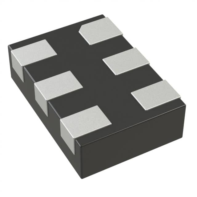
With a typical propagation delay of 1.8 ns at 5.0V, this buffer is suitable for high-speed digital logic applications. It offers a balanced output source and sink capability of 24 mA. The NLVX2G16AMUTCG is available in an ultra-small 6-UDFN package, measuring 1.45x1 mm, making it ideal for space-constrained designs. The component is Pb-Free and Halogen Free.
This dual buffer is well-suited for various digital interface and signal conditioning tasks where reliable high-speed switching is required. Its robust input/output structure and wide operating voltage range make it a versatile choice for modern electronic systems.
| Qty | Low | High |
|---|---|---|
| 1+ | $1.20 | $1.20 |
Estimated market price range - modelled values for guidance only, not live distributor offers.
The operating voltage range is 1.65 V to 5.5 V.
The package is 6-UDFN (1.45 mm x 1.0 mm) for surface mount.
The operating temperature range is -55°C to +125°C.
Yes, it is lead-free (Pb-Free) as verified by the manufacturer datasheet.
Yes, it is halogen-free as verified by the manufacturer datasheet.
The typical propagation delay is 1.8 ns at 5.0 V supply.
The output can source or sink 24 mA balanced, with absolute maximum ±50 mA.