

| Distributor | Stock | Pricing | MOQ | PKG | Lead Time | Date Code | On Order Quantity | On Order Delivery | |
|---|---|---|---|---|---|---|---|---|---|
|
445 pcs
|
445 pcs | On Request | 1 | On Request | On Request | On Request | On Request | On Request |
| Category | |
| Manufacturer Name | |
| AEC Qualified | |
| Automotive Grade | |
| Clock Frequency | |
| Current | |
| Function | |
| Halogen Free | |
| Input Capacitance | |
| Max Propagation Delay @ V, Max CL | |
| Mounting Type | |
| Number of Bits per Element | |
| Number of Elements | |
| Operating Temperature | |
| Output Type | |
| SVHC Present | |
| Supplier Device Package | |
| Tape & Reel | |
| Trigger Type | |
| Type | |
| Voltage |
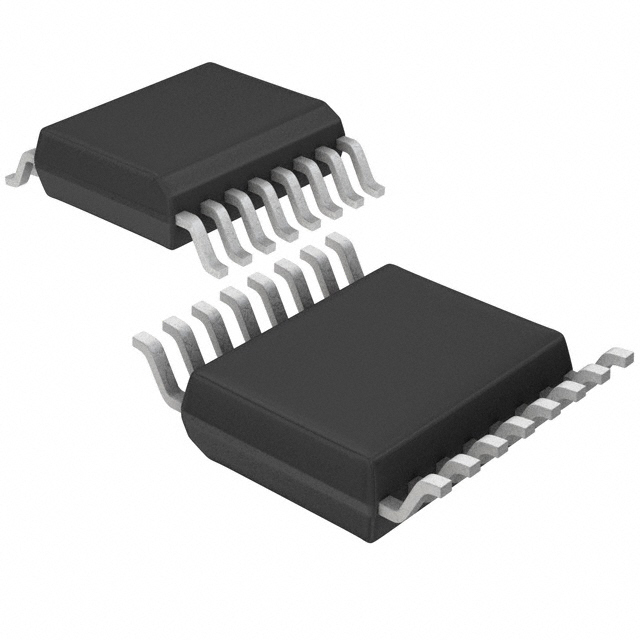
The NLV74HC175ADTR2G is a high-performance silicon-gate CMOS Quad D Flip-Flop manufactured by On Semiconductor. This device features common clock and reset inputs, with separate D inputs for each flip-flop. Information at the D input is transferred to the corresponding Q output on the next positive-going edge of the clock input. The reset input is active-low and asynchronous.
Key electrical specifications include an operating voltage range of 2.0V to 6.0V and a maximum clock frequency of 35 MHz. It offers an output drive capability of 10 LSTTL loads and directly interfaces with CMOS, NMOS, and TTL logic families. The device has a low input current of 4 µA and exhibits high noise immunity characteristic of CMOS devices.
This flip-flop is supplied in a 16-TSSOP surface mount package. It operates within a temperature range of -55°C to 125°C (TA). The device is designed for applications requiring reliable digital logic functions with common clock and reset control.
| Qty | Low | High |
|---|---|---|
| 1+ | $0.86 | $0.86 |
Estimated market price range - modelled values for guidance only, not live distributor offers.
The operating voltage range is 2.0V to 6.0V.
The device is available in a 16-TSSOP surface mount package (0.173", 4.40mm width).
The operating temperature range is -55°C to 125°C.
The maximum clock frequency is 35 MHz.
The maximum propagation delay is 22 ns at 6V and 50 pF load.
The device has complementary outputs.
The device is positive edge triggered.