

| Distributor | Stock | Pricing | MOQ | PKG | Lead Time | Date Code | On Order Quantity | On Order Delivery | |
|---|---|---|---|---|---|---|---|---|---|
|
2,386 pcs
|
2386 pcs | On Request | 1 | On Request | On Request | On Request | On Request | On Request |
| Category | |
| Manufacturer Name | |
| Current | |
| Input Type | |
| Junction Temperature | |
| Logic Type | |
| Mounting Type | |
| Number of Bits per Element | |
| Number of Elements | |
| Operating Temperature | |
| Operating Voltage | |
| Output Current | |
| Output Type | |
| Quiescent Current | |
| Supplier Device Package | |
| Tape & Reel | |
| Voltage |
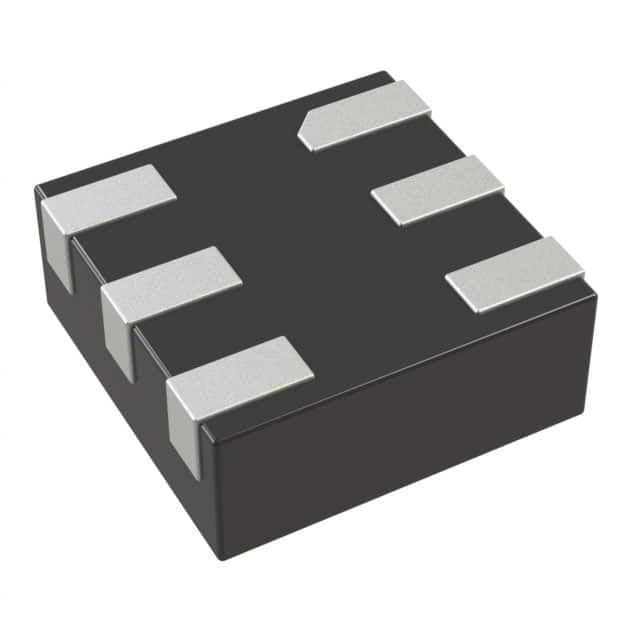
The NLU2G17CMUTCG is an advanced, high-speed CMOS dual non-inverting Schmitt-trigger buffer offered by ON Semiconductor. This component is designed for applications requiring noise immunity enhancement or waveform squaring. It features a wide operating supply voltage range from 1.65V to 5.5V, making it versatile for various system designs.
The device operates across a broad temperature range of -55°C to 125°C (TA), ensuring reliable performance in diverse environmental conditions. Key electrical characteristics include a low quiescent current of 1 µA and output currents of 8mA, 8mA. The input logic levels are defined with a low threshold between 0.9V and 1.65V, and a high threshold between 2.2V and 3.85V, characteristic of Schmitt-trigger inputs.
Packaged in a compact 6-UDFN (1x1) surface-mount form factor, the NLU2G17CMUTCG is suitable for space-constrained applications. The datasheet also specifies maximum ratings including a DC supply voltage up to 7.0V and input/output voltages up to 7.0V, with overvoltage tolerant input and output pins. It is also noted as a Pb-Free device.
This buffer is ideal for digital signal conditioning, interfacing between different logic levels, and improving signal integrity in noisy environments. Its small footprint and robust electrical characteristics make it a valuable component for modern electronic designs.
| Qty | Low | High |
|---|---|---|
| 1+ | $1.20 | $1.20 |
Estimated market price range - modelled values for guidance only, not live distributor offers.
The NLU2G17CMUTCG operates with a supply voltage range of 1.65V to 5.5V.
The NLU2G17CMUTCG is available in a 6-UDFN (1x1) package.
The NLU2G17CMUTCG has an operating temperature range of -55°C to 125°C.
The typical propagation delay is 4.0 ns when VCC is 5.0 V.
The maximum quiescent current for the NLU2G17CMUTCG is 1 µA.
The NLU2G17CMUTCG features Schmitt Trigger inputs.
The NLU2G17CMUTCG has a Push-Pull output type.