

| Distributor | Stock | Pricing | MOQ | PKG | Lead Time | Date Code | On Order Quantity | On Order Delivery | |
|---|---|---|---|---|---|---|---|---|---|
|
51,000 pcs
|
51000 pcs | On Request | 1 | On Request | On Request | On Request | On Request | On Request |
| Category | |
| Manufacturer Name | |
| Current | |
| Logic Type | |
| Max Propagation Delay @ V, Max CL | |
| Mounting Type | |
| Number of Circuits | |
| Number of Inputs | |
| Operating Temperature | |
| Supplier Device Package | |
| Supplier Package | |
| Voltage |
The NLU2G04CMUTCG is a high-speed CMOS dual inverter from ON Semiconductor, designed for applications requiring compact logic solutions. This device features overvoltage tolerant input and output pins, providing protection up to 7.0 V regardless of the supply voltage.
Key electrical characteristics include a wide operating supply voltage range from 1.65V to 5.5V. The maximum propagation delay is 7.5ns at 5V with a 50pF load, and it exhibits high speed with a typical propagation delay of 3.5ns at 5.0V. Power dissipation is low, with a maximum quiescent current of 1µA at 25°C.
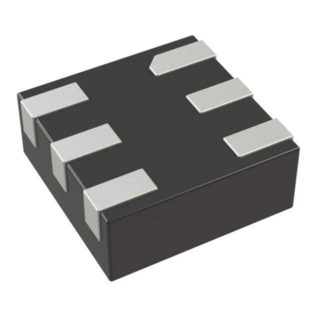
The device operates across a broad temperature range of -55°C to 125°C. It is supplied in a compact 6-UDFN (1x1) surface-mount package, making it suitable for space-constrained designs. The NLU2G04CMUTCG is also Pb-Free.
This dual inverter is designed for general-purpose logic applications where high speed, low power consumption, and small footprint are critical.
| Qty | Low | High |
|---|---|---|
| 1+ | $0.22 | $0.22 |
Estimated market price range - modelled values for guidance only, not live distributor offers.
The supply voltage range is 1.65V to 5.5V.
The device is housed in a 6-UDFN (1x1mm) surface-mount package.
The operating temperature range is -55°C to 125°C.
Maximum propagation delay is 7.5ns at 5V with 50pF load; typical is 3.5ns at 5V.
It contains two independent inverter circuits.
Yes, it is lead-free (Pb-Free) as per the datasheet.
The maximum output source/sink current is ±12.5 mA.