Ready to onboard?
Are you ready to join DistyParts and
grow your business?


| Distributor | Stock | Pricing | MOQ | PKG | Lead Time | Date Code | On Order Quantity | On Order Delivery | |
|---|---|---|---|---|---|---|---|---|---|
|
96,000 pcs
|
96000 pcs | On Request | 1 | On Request | On Request | On Request | On Request | On Request |
| Category | |
| Manufacturer Name | |
| Current | |
| High speed | |
| Input Voltage | |
| Logic Type | |
| Low power dissipation | |
| Mounting Type | |
| Number of Bits per Element | |
| Number of Elements | |
| Operating Temperature | |
| Output Type | |
| Output Voltage (@ Active-Mode (High or Low State) | |
| Output Voltage (@ Power-Down Mode (VCC = 0 V) | |
| Output Voltage (@ Tri-State Mode) | |
| Supplier Device Package | |
| Voltage |
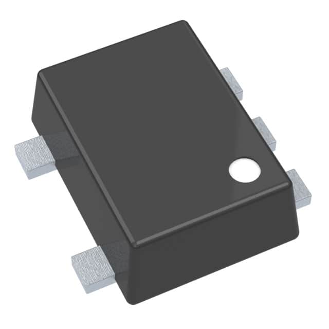
The NL17SG07P5T5G is a single non-inverting buffer from ON Semiconductor designed for low-voltage logic applications. It operates over a wide supply voltage range of 0.9V to 3.6V, making it suitable for battery-powered and portable devices. The device features a typical propagation delay of 2.5ns at VCC=3.0V and CL=15pF, ensuring high-speed signal buffering. With a maximum quiescent current of only 0.5µA at 25°C, it minimizes power consumption in standby or active modes.
The input voltage range extends from -0.5V to 4.3V, and output voltage ranges vary by operating mode: active mode allows -0.5V to VCC+0.5V, while tri-state and power-down modes support -0.5V to 4.3V. The buffer is housed in a compact SOT953 surface-mount package, ideal for space-constrained designs. This device is commonly used in low-voltage logic systems, signal conditioning, and interface buffering in consumer electronics, IoT devices, and industrial controls.
| Qty | Low | High |
|---|---|---|
| 1+ | $1.20 | $1.20 |
Estimated market price range - modelled values for guidance only, not live distributor offers.
The operating voltage range is 0.9V to 3.6V.
The typical propagation delay is 2.5ns at VCC=3.0V and CL=15pF.
The maximum quiescent current is 0.5µA at TA=25°C.
The input voltage range is -0.5V to 4.3V.
In active mode, -0.5V to VCC+0.5V; in tri-state mode, -0.5V to 4.3V; in power-down mode (VCC=0V), -0.5V to 4.3V.