

| Distributor | Stock | Pricing | MOQ | PKG | Lead Time | Date Code | On Order Quantity | On Order Delivery | |
|---|---|---|---|---|---|---|---|---|---|
|
1,722 pcs
|
1722 pcs | On Request | 1 | On Request | On Request | 14+ | On Request | On Request |
| Category | |
| Manufacturer Name | |
| Applications | |
| Lead Spacing | |
| Mounting Type | |
| Power Dissipation | |
| Supplier Device Package | |
| Voltage |
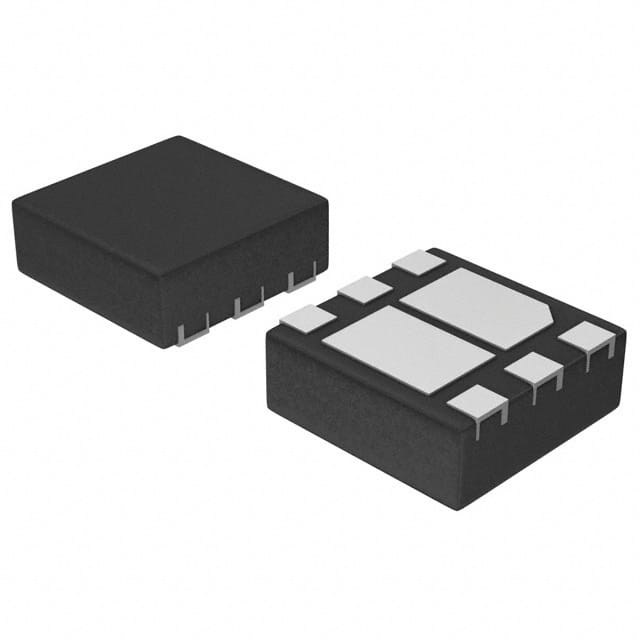
The NIS1050MNTBG from On Semiconductor is a specialized interface integrated circuit designed for protection applications in PMICs. It is targeted at the latest generation of PMICs used in mobile phones and UMPC chipsets.
This device includes a highly stable low-current LDO and a low impedance N-Channel MOSFET. The LDO provides a low current, five-volt supply to the PMIC, while the NFET acts as the external pass element for the Over-Voltage Protection (OVP) circuit. These stages, combined with the internal PMIC, protect the charging circuit from low-impedance overvoltage conditions that can arise from AC/DC or USB supplies.
The NIS1050MNTBG operates with a wide input voltage range of 3V to 30V. It offers lower power dissipation and higher efficiency compared to Zener shunt regulators. The LDO is highly stable across temperature and operates without bypass capacitors.
This protection interface circuit is available in a low-profile 6-lead 2x2mm WDFN6 surface mount package. It is suitable for applications in mobile communications.
| Qty | Low | High |
|---|---|---|
| 1+ | $6.39 | $6.39 |
Estimated market price range - modelled values for guidance only, not live distributor offers.
The operating voltage range for the NIS1050MNTBG is from 3V to 30V.
The NIS1050MNTBG is available in a 6-WDFN Exposed Pad package, specifically a 6-lead 2x2mm WDFN6.
The NIS1050MNTBG is designed for applications in mobile communications.
The maximum continuous drain current at 25°C is 3.7A.
The maximum power dissipation at 25°C is 750mW.