

| Distributor | Stock | Pricing | MOQ | PKG | Lead Time | Date Code | On Order Quantity | On Order Delivery | |
|---|---|---|---|---|---|---|---|---|---|
|
31 pcs
|
31 pcs | On Request | 1 | On Request | On Request | On Request | On Request | On Request |
| Category | |
| Manufacturer Name | |
| Breakdown Voltage Temp. Coefficient | |
| Capacitance Input (@ VDS = 25 V, VGS = 0 V, f = 1.0 MHz) | |
| Charge Gate Total (Maximum @ VDS = 25 V, ID = 2 A) | |
| Configuration | |
| Current | |
| Drain Current, Pulsed | |
| Drain to Source Voltage (Vdss) | |
| Drain-Source Breakdown Voltage | |
| FET Feature | |
| Forward Transconductance | |
| Gate Charge (Qg) (Max) @ Vgs | |
| Gate-Body Leakage Forward | |
| Gate-Body Leakage, Reverse | |
| Gate-Drain Charge | |
| Gate-Source Charge | |
| Gate-Source Voltage | |
| Input Capacitance (Ciss) (Max) @ Vds | |
| Lead Spacing | |
| Mounting Type | |
| On-State Drain Current | |
| Operating and Storage Temperature Range | |
| Output Capacitance | |
| Power | |
| Power Dissipation (Maximum @ Dual operation) | |
| Power Dissipation (Maximum @ Single operation) | |
| Rds On (Max) @ Id, Vgs | |
| Resistance Drain Source On (Maximum @ VGS = 10 V, ID = 3 A) | |
| Resistance Drain Source On (Maximum @ VGS = 10 V, ID = 3 A, TJ =125 °C) | |
| Resistance Drain Source On (Maximum @ VGS = 4.5 V, ID = 1.5 A) | |
| Resistance Drain Source On (Maximum @ VGS = 4.5 V, ID = 1.5 A, TJ =125 °C) | |
| Reverse Transfer Capacitance | |
| Storage Temperature | |
| Supplier Device Package | |
| Tape & Reel | |
| Technology | |
| Thermal Resistance - Junction to Case | |
| Thermal Resistance Junction-to-Ambient | |
| Turn-Off Delay Time | |
| Turn-Off Fall Time | |
| Turn-On Delay Time | |
| Turn-On Rise Time | |
| Vgs(th) (Max) @ Id | |
| Voltage Gate Threshold (Typical @ VDS = VGS, ID = 250 µA) | |
| Voltage Gate Threshold (Typical @ VDS = VGS, ID = 250 µA, TJ =125 °C) | |
| Zero Gate Voltage Drain Current |
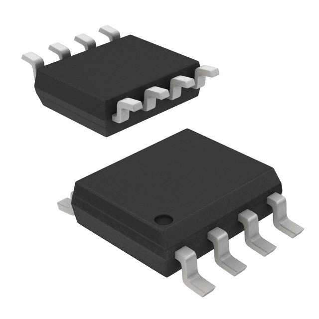
The NDS9955 from ON Semiconductor is a dual N-channel enhancement mode MOSFET. It utilizes a high-density cell design for extremely low on-state resistance (RDS(ON)), making it suitable for applications requiring efficient power handling.
Key electrical specifications include a drain-source voltage (Vdss) of 50V and a continuous drain current (Id) of 3A. The static drain-source on-resistance (RDS(ON)) is rated at a maximum of 130mOhm at 3A and 10V Vgs. The gate threshold voltage (Vgs(th)) is typically 1.7V at 250µA.
This MOSFET is designed for high power and current handling capabilities within a widely used surface mount package. Its technology is tailored for superior switching performance and minimizing on-state power loss, making it ideal for low-voltage applications such as disk drive motor control and battery-powered circuits where fast switching and resistance to transients are important.
The device is housed in an 8-SOIC package, a common surface mount form factor. The mounting type is surface mount, requiring appropriate soldering techniques for reliable integration into electronic designs.
| Qty | Low | High |
|---|---|---|
| 1+ | $0.99 | $0.99 |
Estimated market price range - modelled values for guidance only, not live distributor offers.
The maximum drain-source voltage (Vdss) for the NDS9955 is 50V.
The NDS9955 has a continuous drain current rating of 3A.
The maximum on-resistance (RDS(ON)) for the NDS9955 is 130mOhm at 3A and 10V Vgs.
The NDS9955 is available in an 8-SOIC package.
The operating and storage temperature range for the NDS9955 is -55°C to 150°C.