

| Distributor | Stock | Pricing | MOQ | PKG | Lead Time | Date Code | On Order Quantity | On Order Delivery | |
|---|---|---|---|---|---|---|---|---|---|
|
9,000 pcs
|
9000 pcs | On Request | 1 | On Request | On Request | On Request | On Request | On Request |
| Category | |
| Manufacturer Name | |
| AEC Qualified | |
| Applications | |
| Automotive Grade | |
| Input Voltage | |
| Lead Style | |
| Mounting Type | |
| Number of Outputs | |
| Operating Temperature | |
| Output Voltage | |
| Quiescent Current | |
| Supplier Device Package | |
| Voltage |
The NCV6357MTWDTXG is a configurable, synchronous AOT (Adaptive On-time) buck converter from On Semiconductor, optimized for automotive sub-systems. It supports input voltage ranges from 2.5 V to 5.5 V and can deliver up to 5.0 A of power. The output voltage is programmable from 0.6 V to 3.3 V in 12.5 mV steps.
This device operates at a switching frequency of up to 2.4 MHz, enabling the use of small external components. It features synchronous rectification and automatic PFM/PPWM transitions for improved efficiency, along with low quiescent current. The NCV6357MTWDTXG includes an I2C control interface with interrupt and dynamic voltage scaling support, as well as Enable/VSEL pins and Power Good/Interrupt signaling.
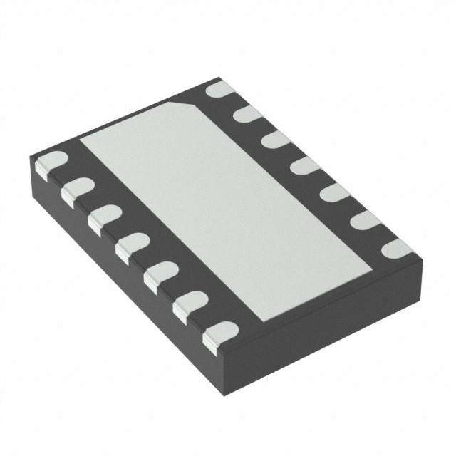
Packaged in a low-profile 3.0 x 4.0 mm DFN-14 package with wettable flanks, it is suitable for surface mount applications. The NCV6357MTWDTXG is AEC-Q100 qualified and PPAP capable, making it ideal for automotive applications such as infotainment, instrumentation, ADAS systems, and automotive POL.
Key electrical specifications include an input voltage range of 2.5 V to 5.5 V and an output current capability of 3.0 A at 105°C and 5.0 A at 85°C. The switching frequency can reach up to 2.4 MHz. The device also features thermal protections and temperature management.
| Qty | Low | High |
|---|---|---|
| 1+ | $0.75 | $0.75 |
Estimated market price range - modelled values for guidance only, not live distributor offers.
The input voltage range is 2.5 V to 5.5 V.
The output voltage is programmable from 0.6 V to 3.3 V in 12.5 mV steps.
The maximum output current is 5.0 A at 85°C and 3.0 A at 105°C.
The operating junction temperature range is -40°C to 125°C.
The device is available in a 14-WDFNW (4x3) package and a 14-WFDFN exposed pad package.
The switching frequency is up to 2.4 MHz.
The quiescent current is 60 µA.