

| Distributor | Stock | Pricing | MOQ | PKG | Lead Time | Date Code | On Order Quantity | On Order Delivery | |
|---|---|---|---|---|---|---|---|---|---|
|
1,842 pcs
|
1842 pcs | On Request | 1 | On Request | On Request | On Request | On Request | On Request | |
|
1,000 pcs
|
1000 pcs | On Request | 1 | On Request | On Request | On Request | On Request | On Request |
| Category | |
| Manufacturer Name | |
| Automotive Grade | |
| Channel Type | |
| Current | |
| Driven Configuration | |
| Gate Type | |
| High Side Voltage | |
| Input Type | |
| Logic Voltage | |
| Mounting Type | |
| Number of Drivers | |
| Operating Temperature | |
| Propagation Delay | |
| Rise | |
| SVHC Present | |
| Supplier Device Package | |
| Supplier Package | |
| Voltage |
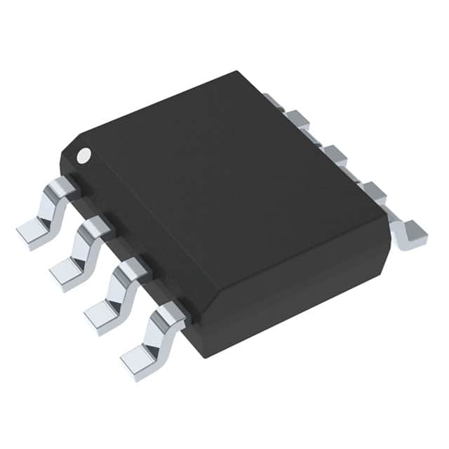
The NCV5183DR2G from On Semiconductor is a high voltage, high current power MOSFET driver. It provides two outputs for direct drive of N-channel power MOSFETs in a half-bridge configuration, utilizing bootstrap techniques for high-side switch drive. This driver is compatible with 3.3V and 5V logic inputs and offers independent channels.
Key electrical specifications include a voltage range up to 600V, dV/dt immunity of 50 V/ns, and a gate drive supply range from 9V to 18V. The output current capability is 4.3A source and 4.3A sink. It features matched propagation delays between channels, typically 120 ns, and includes Under Voltage LockOut (UVLO) protection for both channels. The device also supports an extended allowable negative bridge pin voltage swing to -10V.
Designed for applications such as power supplies for telecom and datacom, half-bridge and full-bridge converters, push-pull converters, high voltage synchronous-buck converters, motor controls, and Class-D audio amplifiers, the NCV5183DR2G is housed in an 8-SOIC package. It is suitable for surface mount applications and operates within a temperature range of -40°C to 125°C (TJ).
| Qty | Low | High |
|---|---|---|
| 1+ | $2.01 | $2.01 |
Estimated market price range - modelled values for guidance only, not live distributor offers.
The operating voltage range for the NCV5183DR2G is from 9 V to 18 V.
The maximum high-side voltage rating for the NCV5183DR2G is 600 V.
The NCV5183DR2G has an output current capability of 4.3 A for both source and sink.
The typical propagation delay for the NCV5183DR2G is 120 ns.
The operating temperature range is -40°C to 125°C (TJ).
This IC includes 2 drivers.
This driver controls N-Channel MOSFET gates.