

| Distributor | Stock | Pricing | MOQ | PKG | Lead Time | Date Code | On Order Quantity | On Order Delivery | |
|---|---|---|---|---|---|---|---|---|---|
|
16,000 pcs
|
16000 pcs | On Request | 1 | On Request | On Request | On Request | On Request | On Request | |
|
1,000 pcs
|
1000 pcs | On Request | 1 | On Request | On Request | On Request | On Request | On Request |
| Category | |
| Manufacturer Name | |
| Approval Agency | |
| Common Mode Transient Immunity (Min) | |
| Current | |
| Lead Spacing | |
| Mounting Type | |
| Number of Channels | |
| Operating Temperature | |
| Propagation Delay tpLH | |
| Pulse Width Distortion (Max) | |
| Rise | |
| Storage Temperature | |
| Supplier Device Package | |
| Tape & Reel | |
| Technology | |
| Voltage | |
| Working Voltage |
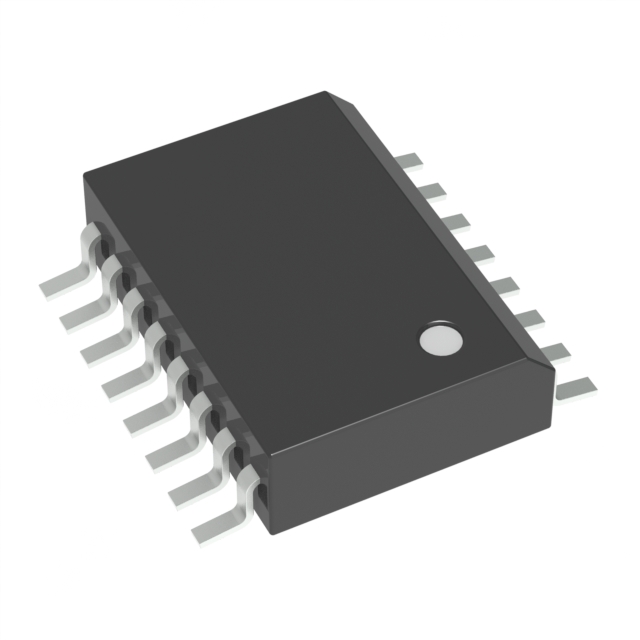
The NCP51561DADWR2G is a high-performance isolated dual-channel gate driver manufactured by onsemi. This device is engineered for rapid switching applications, making it suitable for driving power MOSFETs and SiC MOSFET power switches. It boasts a 4.5A peak source current and a 9A peak sink output current, ensuring robust performance in demanding power management circuits.
Key features include a typical propagation delay of 36ns with excellent delay matching and pulse-width distortion characteristics. The driver offers 5 kVrms internal galvanic isolation and supports a working voltage of up to 1500 VDC, providing enhanced safety and reliability. It can be configured for dual low-side, dual high-side, or half-bridge gate driving, offering flexibility for various power supply designs. The NCP51561DADWR2G also incorporates independent under-voltage lockout (UVLO) protections for both gate drivers and a programmable dead-time adjustment function. It is supplied in a 16-SOIC surface mount package and operates across a wide temperature range of -40°C to 125°C.
Typical applications for this gate driver include motor drives, isolated converters in DC-DC and AC-DC power supplies, server, telecom, and industrial infrastructures, as well as UPS and solar inverters. Its high common mode transient immunity (CMTI > 200 V/ns) ensures stable operation in noisy environments.
| Qty | Low | High |
|---|---|---|
| 1+ | $2.62 | $2.62 |
Estimated market price range - modelled values for guidance only, not live distributor offers.
The NCP51561DADWR2G operates within a temperature range of -40°C to 125°C.
The NCP51561DADWR2G comes in a 16-SOIC (0.295", 7.50mm Width) package.
The NCP51561DADWR2G provides 5 kVrms isolation.
The gate driver has a 4.5 A peak source current and a 9 A peak sink current.
The typical propagation delay for the NCP51561DADWR2G is 36 ns.
The device supports a working voltage of up to 1500 VDC.
The common mode transient immunity (CMTI) is greater than 200 V/ns.