

| Distributor | Stock | Pricing | MOQ | PKG | Lead Time | Date Code | On Order Quantity | On Order Delivery | |
|---|---|---|---|---|---|---|---|---|---|
|
1,918 pcs
|
1918 pcs | On Request | 1 | On Request | On Request | 2010+ | On Request | On Request |
| Category | |
| Manufacturer Name | |
| Channel Type | |
| Driven Configuration | |
| Gate Type | |
| High Side Voltage | |
| Input Type | |
| Lead Style | |
| Logic Voltage | |
| Mounting Type | |
| Number of Drivers | |
| Operating Temperature | |
| Propagation Delay | |
| Rise | |
| SVHC Present | |
| Supplier Device Package | |
| Supplier Package | |
| Tape & Reel | |
| Voltage |
The NCP3418BDR2G from ON Semiconductor is a single-phase, 12V MOSFET gate driver designed for synchronous buck converters. It features dual outputs optimized for driving both high-side and low-side power MOSFETs.
This driver is capable of handling a 3000 pF load with a 25 ns propagation delay and a 20 ns transition time. It offers a wide operating voltage range, allowing optimization of the MOSFET gate drive voltage for maximum efficiency. The internal adaptive nonoverlap circuitry prevents simultaneous conduction, reducing switching losses.
The floating top driver design accommodates boost voltages up to 30V, with transient voltages up to 35V. The Output Disable (OD) pin can drive both gate outputs low. An Undervoltage Lockout function ensures both driver outputs are low when the supply voltage is insufficient, and a Thermal Shutdown function provides overtemperature protection.
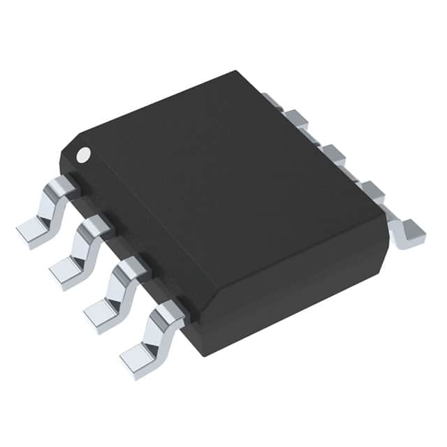
The NCP3418BDR2G is supplied in an 8-SOIC package suitable for surface mounting. It is Pb-Free and compliant with VRM10.x and VRM11.x specifications.
| Qty | Low | High |
|---|---|---|
| 1+ | $2.01 | $2.01 |
Estimated market price range - modelled values for guidance only, not live distributor offers.
4.6V to 13.2V.
8-SOIC surface-mount package.
0°C to 150°C (junction temperature).
2 channels.
N-Channel MOSFETs in a half-bridge configuration.
25ns.
30V.