

| Distributor | Stock | Pricing | MOQ | PKG | Lead Time | Date Code | On Order Quantity | On Order Delivery | |
|---|---|---|---|---|---|---|---|---|---|
|
14,185 pcs
|
14185 pcs | On Request | 1 | On Request | On Request | On Request | On Request | On Request |
| Category | |
| Manufacturer Name | |
| Applications | |
| Mounting Type | |
| Output Voltage | |
| Propagation Delay | |
| Supplier Device Package | |
| Type |
The NBSG16MNR2G from ON Semiconductor is a high-performance SiGe differential receiver/driver targeted for demanding high-frequency applications. It provides superior bandwidth and reduced EMI compared to older devices.
This transceiver IC features internal 50 Ohm termination resistors and supports a wide range of input logic levels including NECL, PECL, HSTL, LVTTL, LVCMOS, CML, and LVDS. The outputs are RSECL (Reduced Swing ECL) with a 400 mV peak-to-peak differential output level.
Key electrical specifications include a maximum input clock frequency exceeding 12 GHz and a maximum input data rate over 12 Gb/s. Typical propagation delay is 120 ps, with rise and fall times of 40 ps. The device operates with VCC from 2.375 V to 3.465 V (VEE = 0 V) for RSPECL outputs, or VCC = 0 V with VEE from -2.375 V to -3.465 V for RSNECL outputs.
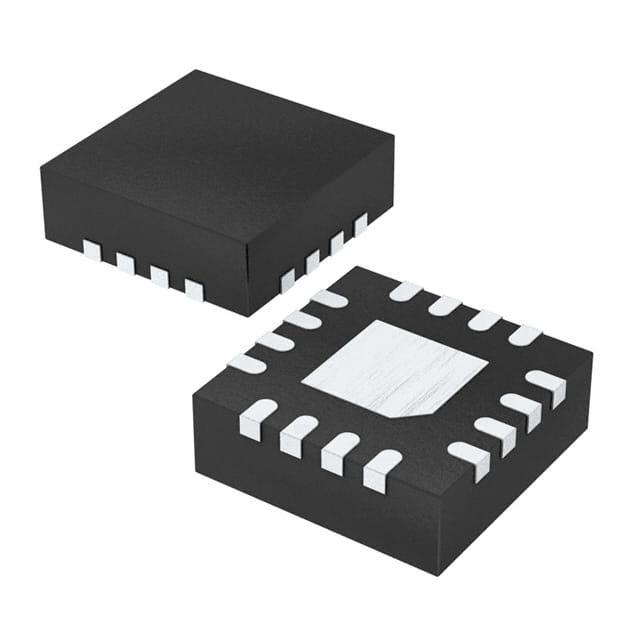
Packaged in a 16-QFN (3x3) with an exposed pad, the NBSG16MNR2G is suitable for surface mount applications. It also features internally generated VBB and VMM reference voltage outputs, which can be used for single-ended inputs or AC coupling. Pb-free packages are available.
| Qty | Low | High |
|---|---|---|
| 1+ | $0.75 | $0.75 |
Estimated market price range - modelled values for guidance only, not live distributor offers.
The maximum input clock frequency is greater than 12 GHz.
The maximum input data rate is greater than 12 Gb/s.
The typical propagation delay is 120 ps.
The typical rise and fall times are 40 ps.
The RSECL output level is 400 mV peak-to-peak, differential only.
Yes, it has internal 50 Ohm input termination resistors.
The operating voltage range for RSPECL output is VCC = 2.375 V to 3.465 V with VEE = 0 V.