

| Distributor | Stock | Pricing | MOQ | PKG | Lead Time | Date Code | On Order Quantity | On Order Delivery | |
|---|---|---|---|---|---|---|---|---|---|
|
4,848 pcs
|
4848 pcs | On Request | 1 | On Request | On Request | On Request | On Request | On Request |
| Category | |
| Manufacturer Name | |
| Differential | |
| Frequency | |
| Input | |
| Mounting Type | |
| Number of Circuits | |
| Operating Temperature | |
| Output | |
| Propagation Delay | |
| Ratio | |
| Supplier Device Package | |
| Supplier Package | |
| Tape & Reel | |
| Type | |
| Voltage |
The NB7V586MMNR4G from ON Semiconductor is a high-performance clock/data distribution chip designed for demanding applications. This device integrates a 2:1 differential input multiplexer with an input select pin, allowing flexible signal routing. It provides six identical differential CML output copies, configured as three banks of two pairs, each capable of being powered by 1.2V or 1.8V supplies.
Optimized for low output skew and minimal jitter, the NB7V586MMNR4G supports data rates exceeding 10 Gb/s and clock frequencies above 6 GHz. Key electrical characteristics include a typical propagation delay of 175 ps and rise/fall times of 50 ps. The inputs accept differential LVPECL, CML, or LVDS levels with internal 50 Ohm termination, while the CML outputs feature internal 50 Ohm source terminations.
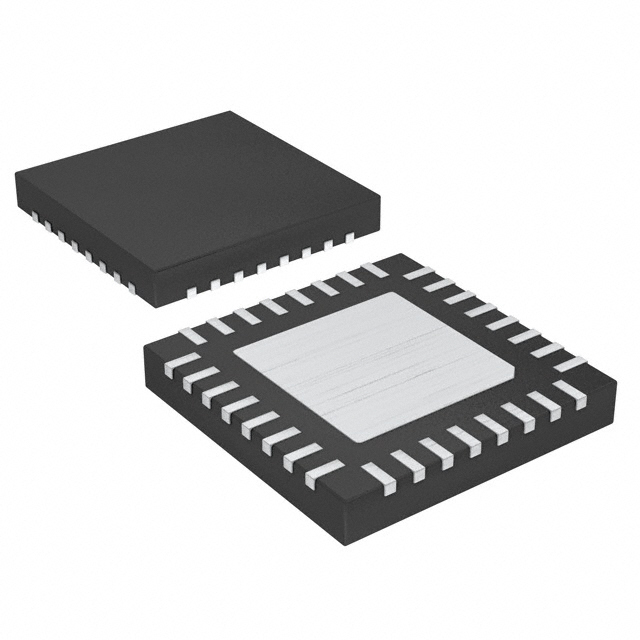
This buffer is housed in a compact 5x5 mm 32-pin QFN package, suitable for surface mounting. Its design makes it ideal for SONET, GigE, Fiber Channel, and backplane clock/data distribution applications. The device operates within a voltage range of 1.71V to 1.89V and an ambient temperature range of -40°C to 85°C.
| Qty | Low | High |
|---|---|---|
| 1+ | $4.44 | $4.44 |
Estimated market price range - modelled values for guidance only, not live distributor offers.
The operating voltage range is 1.71V to 1.89V.
The NB7V586MMNR4G is supplied in a 32-QFN (5x5) package.
The operating temperature range is -40°C to 85°C.
The maximum input clock frequency is greater than 6 GHz typical.
The low skew outputs have a maximum of 20 ps.