

| Distributor | Stock | Pricing | MOQ | PKG | Lead Time | Date Code | On Order Quantity | On Order Delivery | |
|---|---|---|---|---|---|---|---|---|---|
|
2,337 pcs
|
2337 pcs | On Request | 1 | On Request | On Request | On Request | On Request | On Request |
| Category | |
| Manufacturer Name | |
| Clock Frequency | |
| Current | |
| Function | |
| Max Propagation Delay @ V, Max CL | |
| Mounting Type | |
| Number of Bits per Element | |
| Number of Elements | |
| Operating Temperature | |
| Operating Voltage | |
| Output Type | |
| Supplier Device Package | |
| Trigger Type | |
| Type | |
| Voltage |
The NB7V52MMNG from ON Semiconductor is a high-performance differential D flip-flop designed for advanced clock management applications. This device features a differential asynchronous Reset and CML outputs, capable of handling input clock frequencies exceeding 10 GHz and input data rates over 10 Gb/s.
The flip-flop incorporates multi-level inputs with internal 50 Ohm termination resistors, supporting LVPECL, CML, and LVDS logic levels. When the clock transitions from low to high, data is transferred to the differential CML outputs. The differential clock inputs also allow for negative edge-triggered operation.
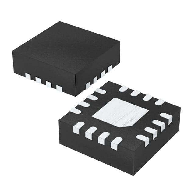
Key electrical characteristics include a typical propagation delay of 200 ps and rise/fall times of 35 ps. The device operates within a voltage range of 1.71V to 2.625V and has a typical output swing of 400 mV. It is housed in a compact 3 mm x 3 mm 16-pin QFN package, suitable for surface mounting.
This component is part of ON Semiconductor's GigaComm family of high-performance clock products. It operates within an ambient temperature range of -40°C to +85°C.
| Qty | Low | High |
|---|---|---|
| 1+ | $0.86 | $0.86 |
Estimated market price range - modelled values for guidance only, not live distributor offers.
The operating voltage range is 1.71 V to 2.625 V.
The NB7V52MMNG is available in a 16-QFN (3x3 mm) package and a 16-VFQFN exposed pad package.
The ambient operating temperature range is -40°C to +85°C.
The maximum clock frequency is greater than 10 GHz.
The maximum input data rate is greater than 10 Gb/s.
The typical random clock jitter is less than 0.8 ps RMS.
The typical supply current is 110 mA.