

| Distributor | Stock | Pricing | MOQ | PKG | Lead Time | Date Code | On Order Quantity | On Order Delivery | |
|---|---|---|---|---|---|---|---|---|---|
|
20,500 pcs
|
20500 pcs | On Request | 1 | On Request | On Request | On Request | On Request | On Request |
| Category | |
| Manufacturer Name | |
| Logic Type | |
| Mounting Type | |
| Number of Circuits | |
| Number of Inputs | |
| Operating Temperature | |
| Output Type | |
| Propagation Delay | |
| Schmitt Trigger Input | |
| Supplier Device Package | |
| Supplier Package | |
| Voltage |
The NB7L86AMNHTBG is a high-performance, multi-function differential logic gate from On Semiconductor, part of the GigaComm /C0116 family. This device can be configured as an AND/NAND, OR/NOR, XOR/XNOR, or a 2:1 MUX, providing significant design flexibility.
It features a maximum input clock frequency exceeding 8 GHz and a maximum input data rate over 8 Gb/s, with a typical propagation delay of 165 ps and rise/fall times of 40 ps. The device supports selectable output swing levels, ranging from 0 mV to 800 mV peak-to-peak, and operates with a supply voltage range of 2.375 V to 3.465 V for PECL output.
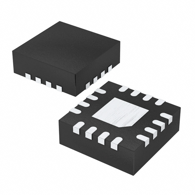
Differential inputs incorporate internal 50 Ohm termination resistors and accept various logic levels including NECL, PECL, LVCMOS/LVTTL, CML, or LVDS. The NB7L86AMNHTBG is housed in a compact 3x3 mm 16-pin QFN package, suitable for surface mounting. Input default circuitry ensures stable outputs under open input conditions.
This Pb-Free device is designed for applications requiring high-speed signal integrity and configurable logic functions.
| Qty | Low | High |
|---|---|---|
| 1+ | $0.39 | $0.39 |
Estimated market price range - modelled values for guidance only, not live distributor offers.
For PECL output, VCC = 2.375 V to 3.465 V with VEE = 0 V. For NECL output, VCC = 0 V with VEE = -2.375 V to -3.465 V.
The device is supplied in a 16-VFQFN exposed pad package, also designated as 16-QFN (3x3), for surface-mount assembly.
The operating temperature range is -40°C to 85°C.
The maximum input clock frequency is greater than 8 GHz typical.
The maximum input data rate is greater than 8 Gb/s typical.
Typical propagation delay is 165 ps.
Output swing can be selected as 0, 200, 400, 600, or 800 mV peak-to-peak.