

| Distributor | Stock | Pricing | MOQ | PKG | Lead Time | Date Code | On Order Quantity | On Order Delivery | |
|---|---|---|---|---|---|---|---|---|---|
|
5,745 pcs
|
5745 pcs | On Request | 1 | On Request | On Request | On Request | On Request | On Request |
| Category | |
| Manufacturer Name | |
| Differential | |
| Frequency | |
| Input | |
| Mounting Type | |
| Number of Circuits | |
| Operating Temperature | |
| Output | |
| Propagation Delay | |
| Ratio | |
| Supplier Device Package | |
| Supplier Package | |
| Tape & Reel | |
| Type | |
| Voltage |
The NB6L611MNG from ON Semiconductor is a high-performance 1:2 differential clock or data fanout buffer. Designed for demanding clock distribution applications, it supports input clock frequencies exceeding 4.0 GHz.
This buffer features internal 50 Ohm termination resistors on its differential inputs, which can accept various logic levels including LVPECL, CML, LVDS, LVCMOS, and LVTTL. It offers a typical propagation delay of 280 ps and rise/fall times of 100 ps, with a maximum RMS clock jitter of 0.5 ps. The device provides differential LVPECL outputs with a typical amplitude of 780 mV.
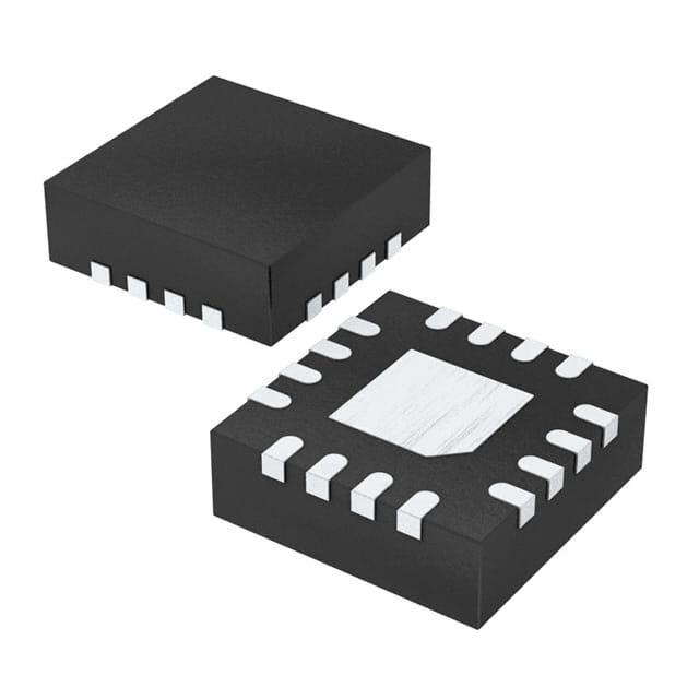
The NB6L611MNG operates within an LVPECL voltage range of 2.375 V to 3.63 V (VEE = 0 V) or an NECL range of -2.375 V to -3.63 V (VCC = 0 V). It is housed in a compact 3x3 mm 16-pin QFN package with an exposed pad, suitable for surface mounting. The operating ambient temperature range is -40°C to +85°C.
This buffer is part of the ECLinPS MAX™ family, offering functional compatibility with existing 2.5 V / 3.3 V LVEL, LVEP, EP, and SG devices. An integrated VREFAC reference output is available for rebias applications.
| Qty | Low | High |
|---|---|---|
| 1+ | $5.33 | $5.33 |
Estimated market price range - modelled values for guidance only, not live distributor offers.
The input clock frequency for the NB6L611MNG is greater than 4.0 GHz.
The typical propagation delay is 280 ps, and the typical rise and fall times are 100 ps.
For LVPECL operation, the voltage range is 2.375 V to 3.63 V with VEE = 0 V. For NECL operation, the range is -2.375 V to -3.63 V with VCC = 0 V.
The operating ambient temperature range is -40°C to +85°C.
The NB6L611MNG is supplied in a 16-QFN (3x3 mm) package with an exposed pad.
The differential inputs can accept LVPECL, CML, LVDS, LVCMOS, or LVTTL logic levels.
The RoHS status is RoHS3 Compliant.