

| Distributor | Stock | Pricing | MOQ | PKG | Lead Time | Date Code | On Order Quantity | On Order Delivery | |
|---|---|---|---|---|---|---|---|---|---|
|
4,920 pcs
|
4920 pcs | On Request | 1 | On Request | On Request | On Request | On Request | On Request |
| Category | |
| Manufacturer Name | |
| Differential | |
| Frequency | |
| Input | |
| Mounting Type | |
| Number of Circuits | |
| Operating Temperature | |
| Output | |
| Propagation Delay | |
| Ratio | |
| Storage Temperature | |
| Supplier Device Package | |
| Tape & Reel | |
| Type | |
| Voltage |
The NB6L11SMNG from On Semiconductor is a versatile 1:2 differential clock or data receiver and fanout buffer. It accepts AnyLevel™ input signals including LVPECL, CML, LVCMOS, LVTTL, or LVDS, and translates them to two identical LVDS outputs. This device is capable of operating at input clock frequencies greater than 2.0 GHz and input data rates exceeding 2.5 Gb/s.
Key electrical characteristics include a typical propagation delay of 380 ps and typical rise and fall times of 120 ps. It features a wide input common mode range and integrated 50 Ohm termination resistors. The NB6L11SMNG operates from a single 2.5 V power supply (±5%) and is suitable for applications such as SONET, GigE, Fiber Channel, and backplane clock distribution.
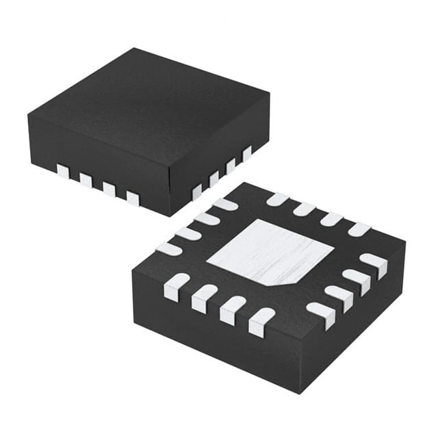
This buffer/translator is housed in a compact 16-QFN (3x3 mm) package with a surface mount type. It is designed for operation across a temperature range of -40°C to 85°C. The device is Pb-Free and meets RoHS3 compliance standards.
| Qty | Low | High |
|---|---|---|
| 1+ | $4.44 | $4.44 |
Estimated market price range - modelled values for guidance only, not live distributor offers.
The input clock frequency is greater than 2.0 GHz.
It accepts AnyLevel™ input signals including LVPECL, CML, LVCMOS, LVTTL, or LVDS.
The output signal type is LVDS.
The operating voltage is 2.5V.
The operating temperature range is -40°C to 85°C.
It is supplied in a 16-QFN (3x3 mm) package.