

| Distributor | Stock | Pricing | MOQ | PKG | Lead Time | Date Code | On Order Quantity | On Order Delivery | |
|---|---|---|---|---|---|---|---|---|---|
|
154 pcs
|
154 pcs | On Request | 1 | On Request | On Request | 13+ | On Request | On Request | |
|
5 pcs
|
5 pcs | On Request | 1 | On Request | On Request | On Request | On Request | On Request |
| Category | |
| Manufacturer Name | |
| AEC Qualified | |
| Automotive Grade | |
| Differential | |
| Frequency | |
| Industrial Grade | |
| Input | |
| Lead Spacing | |
| Medical Grade | |
| Military Grade | |
| Mounting Type | |
| Number of Circuits | |
| Operating Temperature | |
| Output | |
| Ratio | |
| Supplier Device Package | |
| Tape & Reel | |
| Type | |
| Voltage |
The NB6L11DR2G is a high-performance clock buffer and translator manufactured by ON Semiconductor. This component is designed to distribute clock signals with a 1:2 ratio, supporting a maximum frequency of 6 GHz. It operates within a supply voltage range of 2.375V to 3.465V and features ECL output.
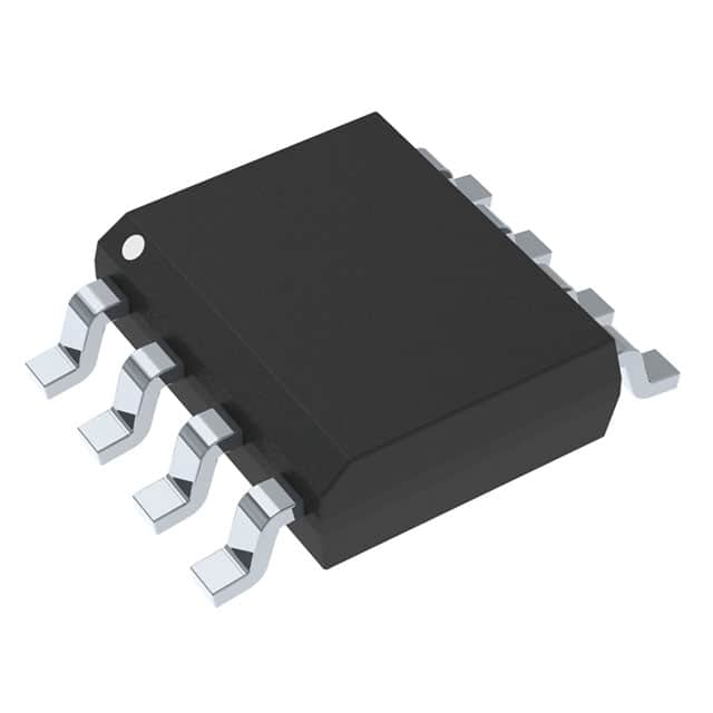
The NB6L11DR2G supports a wide array of input signal types, including CML, LVCMOS, LVDS, LVNECL, LVPECL, and LVTTL, making it versatile for various system designs. It is housed in an 8-SOIC package and is designed for surface mount applications.
This clock buffer is suitable for applications requiring precise clock distribution and signal integrity at high frequencies. Its robust design and broad input compatibility make it a valuable component in complex timing circuits.
| Qty | Low | High |
|---|---|---|
| 1+ | $4.44 | $4.44 |
Estimated market price range - modelled values for guidance only, not live distributor offers.
The operating voltage for the NB6L11DR2G is between 2.375V and 3.465V.
The NB6L11DR2G is available in an 8-SOIC package.
The operating temperature range for the NB6L11DR2G is -40°C to 85°C.
The NB6L11DR2G is RoHS3 Compliant.
The NB6L11DR2G supports a maximum frequency of 6 GHz.
The NB6L11DR2G supports CML, LVCMOS, LVDS, LVNECL, LVPECL, and LVTTL input signals.