

| Distributor | Stock | Pricing | MOQ | PKG | Lead Time | Date Code | On Order Quantity | On Order Delivery | |
|---|---|---|---|---|---|---|---|---|---|
|
738 pcs
|
738 pcs | On Request | 1 | On Request | On Request | On Request | On Request | On Request |
| Category | |
| Manufacturer Name | |
| Logic Type | |
| Mounting Type | |
| Number of Bits | |
| Operating Temperature | |
| Propagation Delay | |
| SVHC Present | |
| Supplier Device Package | |
| Supply Voltage |
The NB4N527SMNG from On Semiconductor is a high-speed logic interface component designed for clock and data signal translation. It is capable of translating various input signal types, including LVPECL, CML, HSTL, LVDS, and LVTTL/LVCMOS, to LVDS outputs.
This device supports maximum input clock frequencies up to 1.5 GHz and maximum input data rates up to 2.5 Gb/s. Key electrical characteristics include a maximum propagation delay of 470 ps, a maximum RMS jitter of 1 ps, and maximum rise/fall times of 140 ps. It operates from a single 3.3V power supply and features a wide input common mode range from GND + 50 mV to VCC - 50 mV. Internal 50 Ohm termination resistors are included for differential or single-ended signals, simplifying external component requirements.
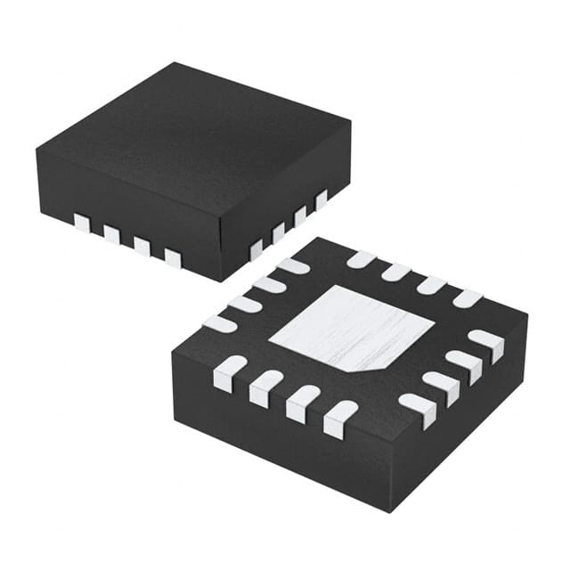
The NB4N527SMNG is housed in a compact 3 mm x 3 mm 16-QFN package, making it suitable for applications where space is a constraint. It is targeted for data, wireless, and telecom applications, as well as high-speed logic interfaces where low jitter and small package size are critical design requirements. The device operates within a temperature range of -40°C to 85°C.
| Qty | Low | High |
|---|---|---|
| 1+ | $0.50 | $0.50 |
Estimated market price range - modelled values for guidance only, not live distributor offers.
The supply voltage range is 3V to 3.6V, with a nominal 3.3V operation.
It is available in a 16-VFQFN exposed pad package (16-QFN 3x3 mm) for surface mount.
The operating temperature range is -40°C to 85°C.
Yes, the NB4N527SMNG is lead-free (Pb-Free) as verified by the datasheet.
The maximum input clock frequency is 1.5 GHz.
The maximum input data rate is 2.5 Gb/s.
The maximum RMS jitter is 1 ps.