

| Distributor | Stock | Pricing | MOQ | PKG | Lead Time | Date Code | On Order Quantity | On Order Delivery | |
|---|---|---|---|---|---|---|---|---|---|
|
12,664 pcs
|
12664 pcs | On Request | 1 | On Request | On Request | On Request | On Request | On Request |
| Category | |
| Manufacturer Name | |
| Differential | |
| Frequency | |
| Input | |
| Input Type | |
| Mounting Type | |
| Number of Circuits | |
| Operating Temperature | |
| Output | |
| Ratio | |
| Supplier Device Package | |
| Tape & Reel | |
| Type | |
| Voltage |
The NB3V8312CMNG from On Semiconductor is an ultra-low jitter, low skew 1:12 fanout buffer. It is capable of distributing 12 clocks from a single LVCMOS/LVTTL input up to a maximum frequency of 250 MHz.
This buffer features separate VDD core and VDDQ output supplies, allowing for flexible voltage configurations and improved power consumption. The outputs can be disabled to a high impedance state via the OE input. Additionally, a synchronous clock enable (CLK_EN) input prevents output glitches during enable/disable transitions.
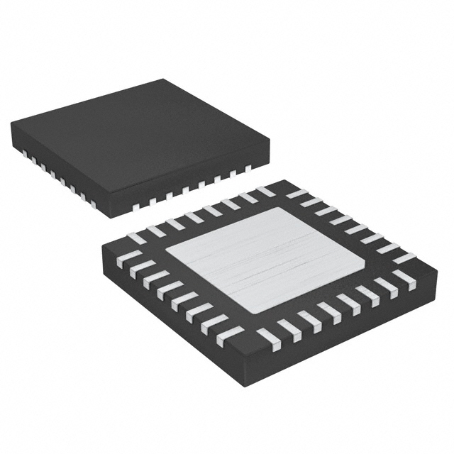
The NB3V8312CMNG is housed in a 32-pin QFN package and is suitable for surface mounting. Its operating temperature range is -40°C to 85°C. This component is well-suited for applications in networking, telecom, server and storage area networking, RRU LO reference distribution, medical, and test equipment.
Key electrical specifications include a maximum clock frequency of 250 MHz, LVCMOS/LVTTL input compatibility, and 12 LVCMOS outputs. The skew between outputs is a maximum of 150 ps. The supply voltage range is 1.6V to 3.465V.
| Qty | Low | High |
|---|---|---|
| 1+ | $4.44 | $4.44 |
Estimated market price range - modelled values for guidance only, not live distributor offers.
The maximum clock frequency is 250 MHz.
It accepts LVCMOS and LVTTL clock inputs.
It provides 12 LVCMOS clock outputs.
The operating temperature range is -40°C to 85°C.
It is supplied in a 32-QFN (5x5) package.
The RoHS status is RoHS3 Compliant.